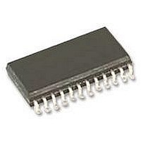
LM2650M-ADJ National Semiconductor, LM2650M-ADJ Datasheet - Page 4

LM2650M-ADJ
Manufacturer Part Number
LM2650M-ADJ
Description
DC/DC CONVERTER, ADJ, 2650, SOIC24
Manufacturer
National Semiconductor
Datasheet
1.LM2650M-ADJ.pdf
(11 pages)
Specifications of LM2650M-ADJ
Primary Input Voltage
18V
No. Of Outputs
1
Output Voltage
16V
Output Current
3A
Voltage Regulator Case Style
SOIC
No. Of Pins
24
Operating Temperature Range
-40°C To +125°C
Svhc
No SVHC
Lead Free Status / RoHS Status
Lead free / RoHS Compliant
Available stocks
Company
Part Number
Manufacturer
Quantity
Price
Company:
Part Number:
LM2650M-ADJ
Manufacturer:
NS
Quantity:
1 438
Company:
Part Number:
LM2650M-ADJ
Manufacturer:
NATIONAL
Quantity:
425
Part Number:
LM2650M-ADJ
Manufacturer:
NS/国半
Quantity:
20 000
Company:
Part Number:
LM2650M-ADJ/NOPB
Manufacturer:
TI
Quantity:
15 540
www.national.com
D
V
V
I
V
T
SS
V
type apply for T
Operating Ratings.
SD
DD
BOOT
HYST
MIN
Electrical Characteristics
Note 1: Absolute Maximum Ratings are limits beyond which damage to the device may occur. Operating Ratings are conditions under which the device operates
correctly. Operating ratings do not imply guaranteed performance limits. For guaranteed performance limits and associated test conditions, see the Electrical
Characteristics.
Note 2: This rating is calculated using the formula P
junction temperature, and
78˚C/W for T
the safe dissipation of more power. See Application Notes on thermal management. The LM2650 actively limits its junction temperature to about 170˚C.
Note 3: For detailed information on soldering plastic small-outline packages, refer to the Packaging Databook published by National Semiconductor Corporation.
Note 4: ESD is applied using the human-body model, a 100pF capacitor discharged through a 1.5k
Note 5: A typical is the center of characterization data taken at T
Note 6: All limits are guaranteed. The guarantee is backed with 100% testing at T
Note 7: V
Note 8: Quiescent current is the total current flowing into the P
nominal switching frequency. I
Note 9: Pulling 100µA out of FREQ ADJ simulates adjusting the oscillator frequency with a 12.5 k
cannot be used at switching frequencies above 250 kHz.
PVIN
Symbol
= 15V, V
REF
Jmax
is measured at SLEEP OUT ADJ.
, T
Minimum Duty Cycle
Internal Rail Voltage
Bootstrap Regulator Voltage
(VRegH)
Soft Start Current
Hysteresis of the Sleep
Comparator (C2 Figure 2 )
V
V
V
V
V
V
T
SLEEP LOGIC
A
J
IL
IH
IL
IH
IL
IH
A
= T
for Thermal Shutdown
and
of SD
of SLEEP LOGIC
of SYNC
of SD
of SLEEP LOGIC
of SYNC
J
JA
JA
= +25˚C. Limits appearing in boldface type apply over the full junction temperature range shown under
QS
is the junction ot ambient thermal resistance of the package. The P
respectively. A
Parameter
includes no such current.
= 0V and V
JA
of 78˚C represents the worst condition of no heat sinking of the M24B small-outline package. Heat sinking allows
SD
DCmax
= 0V unless superseded under Conditions. Typicals and limits appearing in plain
(Continued)
= (T
V
F
I
I
V
VIN
VDD
BOOT
OSC
Jmax
FB
SLEEPLOGIC
A
and V
= T
= V
= 1 mA
− T
Not Adjusted
= 1 mA
J
A
IN
REF
= 25˚C.
) /
pins. I
Conditions
JA
+50 mV,
= 3V
, where P
4
Q
A
includes the current used to drive the gates of the two NMOS power FETs at the
= T
J
DCmax
= 125˚C and statistical correlation for room temperature and cold limits.
is the absolute maximum power dissipation, T
DCmax
resistor connected from FREQ ADJ to GND. The sleep mode
resistor.
rating of 1.28W results from substituting 170˚C, 70˚C and
Typ (Note 5)
170
2.8
4.0
7.5
10
30
Limit (Note 6)
13.5/20.0
3.6/3.4
4.2/4.3
6.5/6.0
0.95
2.10
0.50
1.45
0.9
2.0
10
50
5
Jmax
is the maximum
mV(max)
µA(max)
mV(min)
%(min)
V(max)
V(max)
V(max)
V(max)
V(min)
V(min)
V(min)
V(min)
V(min)
Units
mV
µA
˚C
%
V
V


