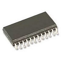
LM2650M-ADJ National Semiconductor, LM2650M-ADJ Datasheet - Page 8

LM2650M-ADJ
Manufacturer Part Number
LM2650M-ADJ
Description
DC/DC CONVERTER, ADJ, 2650, SOIC24
Manufacturer
National Semiconductor
Datasheet
1.LM2650M-ADJ.pdf
(11 pages)
Specifications of LM2650M-ADJ
Primary Input Voltage
18V
No. Of Outputs
1
Output Voltage
16V
Output Current
3A
Voltage Regulator Case Style
SOIC
No. Of Pins
24
Operating Temperature Range
-40°C To +125°C
Svhc
No SVHC
Lead Free Status / RoHS Status
Lead free / RoHS Compliant
Available stocks
Company
Part Number
Manufacturer
Quantity
Price
Company:
Part Number:
LM2650M-ADJ
Manufacturer:
NS
Quantity:
1 438
Company:
Part Number:
LM2650M-ADJ
Manufacturer:
NATIONAL
Quantity:
425
Part Number:
LM2650M-ADJ
Manufacturer:
NS/国半
Quantity:
20 000
Company:
Part Number:
LM2650M-ADJ/NOPB
Manufacturer:
TI
Quantity:
15 540
www.national.com
Operation
The diode D2 is the body diode of Q2. The hysteretic circuit
uses D2 as a rectifier instead of switching Q2 as a synchro-
nous rectifier.
When the load current drops below the prescribed sleep-in
threshold, the LM2650 shuts down the PWM loop and starts
up the hysteretic loop. The hysteretic loop supports light
loads more efficiently because it uses less power to support
its own operation; it uses less bias power because it’s a
simpler loop having less circuit blocks to bias, and it switches
slower, so it incurs lower switching losses.
The hysteretic control loop does not switch at a constant
frequency. Instead, it monitors V
V
the desired output voltage. C2 directs the switching based
on its reading of the feedback voltage. Switching in this
manner yields a regulated voltage consisting of the desired
output voltage and an AC ripple voltage. The magnitude of
the AC component can be approximated using
For example, with V
120mV,
When it starts up, the hysteretic loop turns Q1 on. While Q1
is on, the input power supply charges C
current to the load. Current from the supply reaches C and
the load via the series path provided by Q1 and L1. As the
feedback voltage just surpasses the upper hysteretic thresh-
old of C2, the output of C2 changes from high to low, and HD
responds by pulling the gate of Q1 down turning Q1 off. As
Q1 turns off, L1 generates a negative-going voltage transient
that D2 clamps at just below ground. D2 remains on only
briefly as the current in L1 runs out. While both Q1 and D2
are off, C
OUT
reaches either side of a narrow window centered on
OUT
alone supplies current to the load. As the
(Continued)
OUT
set to 5V, V
OUT
OUT_PP
and switches only when
FIGURE 4. The Typical 90 kHz Application Circuit
OUT
is approximately
and supplies
(4)
(5)
8
feedback voltage just surpasses the lower hysteretic thresh-
old of C2, the output of C2 changes states from low to high,
and DH responds by pulling the gate of Q1 up turning Q1 on
and starting the hysteretic cycle over.
Note that as the load current decreases, it takes increasingly
longer periods for the load current to discharge C
through the hysteretic window, and as the load current in-
creases, the periods become even shorter. It can be seen
from the above observation that the switching frequency of
the hysteretic loop varies as the load varies. The switching
frequency can be approximated using
Here f is the switching frequency in hertz, I is the load current
in amperes, C
V
Typical switching frequencies range anywhere from a few
hertz for very light loads to a few thousand hertz for light
loads bordering on the moderate level.
Application Circuits
Figure 4 is a schematic of the typical application circuit. use
the component values shown in the figure and those con-
tained in Table 1 to build a 5V, 3A, or 3.3V, 3A step-down
DC/DC converter. As with the design of any DC/DC con-
verter, the design of these circuits involved tradeoffs be-
tween efficiency, size, and cost. Here more weight was given
to efficiency than to size as evidenced by the low switching
frequency which keeps switching losses low but pushes the
value and size of the inductor up.
From a smaller circuit, use the component values shown in
Figure 4 and those contained in Table 3 . These circuits trade
slightly higher switching losses for a much smaller inductor.
Note, Figure 4 does not show R
adjust the switching frequency from 90 kHz up to 200 kHz.
Connect R
OUT_PP
is the magnitude of the AC ripple voltage in volts.
FA
between the FREQ ADJ pin and ground.
OUT
is the value of the capacitor in farads, and
DS012848-19
FA
, the resistor required to
OUT
(6)


