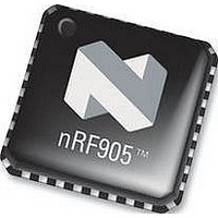
NRF905 NORDIC SEMICONDUCTOR, NRF905 Datasheet - Page 12

NRF905
Manufacturer Part Number
NRF905
Description
IC, TRANSCEIVER, 430 928MHZ, SMD
Manufacturer
NORDIC SEMICONDUCTOR
Datasheet
1.NRF905.pdf
(42 pages)
Specifications of NRF905
Transmitting Current
9mA
Data Rate
50Kbps
Frequency Range
430MHz To 928MHz
Modulation Type
GFSK
Sensitivity Dbm
-100dBm
Rf Ic Case Style
QFN
No. Of Pins
32
Supply Voltage Range
1.9V To 3.6V
Output Power
10dBm
Rohs Compliant
Yes
Lead Free Status / RoHS Status
Lead free / RoHS Compliant
Available stocks
Company
Part Number
Manufacturer
Quantity
Price
Part Number:
NRF905
Manufacturer:
NORDIC
Quantity:
20 000
Company:
Part Number:
NRF905-REEL
Manufacturer:
NORDIC
Quantity:
20 000
Part Number:
NRF905-REEL
Manufacturer:
NORDIC
Quantity:
20 000
Company:
Part Number:
NRF905C
Manufacturer:
NORDIC
Quantity:
10 615
PRODUCT SPECIFICATION
nRF905 Single Chip 433/868/915 MHz Radio Transceiver
5.5
If TX_EN is set high while TRX_CE is kept high, the nRF905 would enter
ShockBurst
registers.
If TRX_CE or TX_EN is changed during an incoming packet, the nRF905 changes
mode immediately and the packet is lost. However, if the MCU is sensing the Address
Match (AM) pin, it knows when the chip is receiving an incoming packet and can
therefore decide whether to wait for the Data Ready (DR) signal or enter a different
mode.
To avoid spurious address matches it is recommended that the address length be 24
bits or higher in length. Small addresses such as 8 or 16 bits can often lead to
statistical failures due to the address being repeated as part of the data packet. This
can be avoided by using a longer address.
Each byte within the address should be unique. Repeating bytes within the address
reduces the effectiveness of the address and increases its susceptibility to noise hence
increasing the packet error rate. The address should also have several level shifts (i.e.
10101100) to reduce the statistical effect of noise and hence reduce the packet error
rate.
Main office: Nordic Semiconductor ASA
Revision: 1.4
Typical ShockBurst
1. ShockBurst
2. After 650 s nRF905 is monitoring the air for incoming communication.
3. When the nRF905 senses a carrier at the receiving frequency, Carrier
4. When a valid address is received, Address Match (AM) pin is set high.
5. When a valid packet has been received (correct CRC found), nRF905
6. MCU sets the TRX_CE low to enter standby mode (low current mode).
7. MCU can clock out the payload data at a suitable rate via the SPI interface.
8. When all payload data is retrieved, nRF905 sets Data Ready (DR) and
9. The chip is now ready for entering ShockBurst
Detect (CD) pin is set high.
removes the preamble, address and CRC bits, and the Data Ready (DR)
pin is set high.
Address Match (AM) low again.
power down mode.
TM
TX and start a transmission according to the present contents in the SPI-
TM
RX is selected by setting TRX_CE high and TX_EN low.
TM
- Vestre Rosten 81, N-7075 Tiller, Norway
RX
Page 12 of 42
TM
- Phone +4772898900 -Fax +4772898989
RX, ShockBurst
TM
June 2006
TX or


