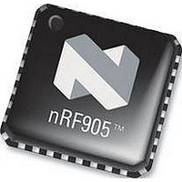
NRF905 NORDIC SEMICONDUCTOR, NRF905 Datasheet - Page 27

NRF905
Manufacturer Part Number
NRF905
Description
IC, TRANSCEIVER, 430 928MHZ, SMD
Manufacturer
NORDIC SEMICONDUCTOR
Datasheet
1.NRF905.pdf
(42 pages)
Specifications of NRF905
Transmitting Current
9mA
Data Rate
50Kbps
Frequency Range
430MHz To 928MHz
Modulation Type
GFSK
Sensitivity Dbm
-100dBm
Rf Ic Case Style
QFN
No. Of Pins
32
Supply Voltage Range
1.9V To 3.6V
Output Power
10dBm
Rohs Compliant
Yes
Lead Free Status / RoHS Status
Lead free / RoHS Compliant
Available stocks
Company
Part Number
Manufacturer
Quantity
Price
Part Number:
NRF905
Manufacturer:
NORDIC
Quantity:
20 000
Company:
Part Number:
NRF905-REEL
Manufacturer:
NORDIC
Quantity:
20 000
Part Number:
NRF905-REEL
Manufacturer:
NORDIC
Quantity:
20 000
Company:
Part Number:
NRF905C
Manufacturer:
NORDIC
Quantity:
10 615
PRODUCT SPECIFICATION
nRF905 Single Chip 433/868/915 MHz Radio Transceiver
8.8
PCB Layout and Decoupling Guidelines
nRF905 is an extremely robust RF device due to internal voltage regulators and
requires the minimum of RF layout protocols. However the following design rules
should still be incorporated into the layout design.
A PCB with a minimum of two layers including a ground plane is recommended for
optimum performance. The nRF905 DC supply voltage should be decoupled as close
as possible to the VDD pins with high performance RF capacitors. It is preferable to
mount a large surface mount capacitor (e.g. 4.7 F tantalum) in parallel with the
smaller value capacitors. The nRF905 supply voltage should be filtered and routed
separately from the supply voltages of any digital circuitry.
Long power supply lines on the PCB should be avoided. All device grounds, VDD
connections and VDD bypass capacitors must be connected as close as possible to the
nRF905 IC. For a PCB with a topside RF ground plane, the VSS pins should be
connected directly to the ground plane. For a PCB with a bottom ground plane, the
best technique is to place via holes as close as possible to the VSS pins. A minimum
of one via hole should be used for each VSS pin.
Full swing digital data or control signals should not be routed close to the crystal or
the power supply lines.
A fully qualified RF-layout for the nRF905 and its surrounding components,
including
antennas
and
matching
networks,
can
be
downloaded
from
www.nordicsemi.no.
Main office: Nordic Semiconductor ASA
- Vestre Rosten 81, N-7075 Tiller, Norway
- Phone +4772898900 -Fax +4772898989
Revision: 1.4
Page 27 of 42
June 2006


