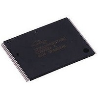
S29GL01GP11FFIR20 Spansion Inc., S29GL01GP11FFIR20 Datasheet - Page 19

S29GL01GP11FFIR20
Manufacturer Part Number
S29GL01GP11FFIR20
Description
Flash - NOR IC
Manufacturer
Spansion Inc.
Datasheet
1.S29GL01GP11FFIR20.pdf
(80 pages)
Specifications of S29GL01GP11FFIR20
Memory Size
1000Mbit
Memory Configuration
128K X 16
Ic Interface Type
CFI, Parallel
Access Time
110ns
Supply Voltage Range
3V To 3.6V
Memory Case Style
TSOP
No. Of Pins
64
Cell Type
NOR
Density
1Gb
Access Time (max)
110ns
Interface Type
Parallel
Boot Type
Not Required
Address Bus
27/26Bit
Operating Supply Voltage (typ)
3/3.3V
Operating Temp Range
-40C to 85C
Package Type
Fortified BGA
Sync/async
Asynchronous
Operating Temperature Classification
Industrial
Operating Supply Voltage (min)
3V
Operating Supply Voltage (max)
3.6V
Word Size
8/16Bit
Number Of Words
128M/64M
Supply Current
110mA
Mounting
Surface Mount
Pin Count
64
Lead Free Status / Rohs Status
Compliant
Available stocks
Company
Part Number
Manufacturer
Quantity
Price
Company:
Part Number:
S29GL01GP11FFIR20
Manufacturer:
SPANSION
Quantity:
1 000
7. Device Operations
7.1
Legend
L = Logic Low = V
Notes
1. Addresses are AMax:A0 in word mode; A
2. If WP# = V
3. D
November 17, 2010 S29GL-P_00_A13
Operation
Read
Write (Program/Erase)
Accelerated Program
Standby
Output Disable
Reset
WP# is at V
IN
or D
OUT
Device Operation Table
IL
IH
, on the outermost sector remains protected. If WP# = V
as required by command sequence, data polling, or sector protect algorithm.
. All sectors are unprotected when shipped from the factory (The Secured Silicon Sector can be factory protected depending on version ordered.)
IL
, H = Logic High = V
Note
This table has been condensed to show sector-related information for an entire device on a single page. Sectors and their address ranges
that are not explicitly listed (such as SA001-SA510) have sector starting and ending addresses that form the same pattern as all other
sectors of that size. For example, all 128 Kb sectors have the pattern xxx0000h-xxxFFFFh.
This section describes the read, program, erase, handshaking, and reset features of the Flash devices.
Operations are initiated by writing specific commands or a sequence with specific address and data patterns
into the command registers (see
occupy any addressable memory location; rather, it is composed of latches that store the commands, along
with the address and data information needed to execute the command. The contents of the register serve as
input to the internal state machine and the state machine outputs dictate the function of the device. Writing
incorrect address and data values or writing them in an improper sequence may place the device in an
unknown state, in which case the system must pull the RESET# pin low or power cycle the device to return
the device to the reading array data mode.
The device must be setup appropriately for each operation.
control pin for any particular operation.
Uniform Sector
64 Kword/
128 Kbyte
V
CC
Size
CE#
±
L
L
L
L
X
0.3 V
IH
, V
HH
Max
OE#
= 11.5–12.5V, X = Don’t Care, A
:A-1 in byte mode.
H
H
X
H
X
L
Sector
Count
128
D a t a
WE#
Table 6.4 S29GL128P Sector & Memory Address Map
H
X
H
X
L
L
S29GL-P MirrorBit
Table 7.1 Device Operations
V
Table 12.1
CC
RESET#
S h e e t
Sector
Range
SA127
SA00
±
H
H
H
H
L
IH
:
0.3 V
, the outermost sector is unprotected. WP# has an internal pull-up; when unconnected,
IN
through
WP#/ACC
= Address In, D
(Note 2)
®
V
Flash Family
X
H
X
X
HH
Address Range (16-bit)
Table
0000000h - 000FFFFh
07F0000 - 7FFFFF
Addresses
IN
12.4). The command register itself does not
(Note 1)
Table 7.1
= Data In, D
A
A
A
X
X
X
IN
IN
IN
:
OUT
describes the required state of each
DQ0–DQ7
(Note 3)
(Note 3)
High-Z
High-Z
High-Z
= Data Out
D
OUT
BYTE#= V
Sector Starting Address
(Note 3)
(Note 3)
Sector Ending Address
High-Z
High-Z
High-Z
D
OUT
DQ8–DQ15
IH
Notes
BYTE#= V
DQ15 = A-1
DQ8–DQ14
= High-Z,
High-Z
High-Z
High-Z
IL
19


