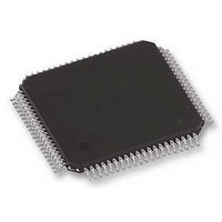
SAK-C164CI-8E25M Infineon Technologies, SAK-C164CI-8E25M Datasheet - Page 6

SAK-C164CI-8E25M
Manufacturer Part Number
SAK-C164CI-8E25M
Description
IC, 16BIT MCU, 64K OTP, MQFP80, 164
Manufacturer
Infineon Technologies
Datasheet
1.SAK-C164CI-8E25M.pdf
(53 pages)
Specifications of SAK-C164CI-8E25M
Core Size
16bit
No. Of I/o's
59
Program Memory Size
64KB
Ram Memory Size
4KB
Cpu Speed
25MHz
Oscillator Type
External Only
No. Of Timers
5
Digital Ic Case Style
MQFP
Supply Voltage
RoHS Compliant
Controller Family/series
C164CI
Peripherals
ADC
Rohs Compliant
Yes
Available stocks
Company
Part Number
Manufacturer
Quantity
Price
Company:
Part Number:
SAK-C164CI-8E25M
Manufacturer:
INFINEON
Quantity:
49
Company:
Part Number:
SAK-C164CI-8E25M DB
Manufacturer:
Infineon Technologies
Quantity:
10 000
Pin Definitions and Functions
Symbol
P5.0 –
P5.7
P3.4,
P3.6,
P3.8 –
P3.13,
P3.15
P4.0 –
P4.3
P4.5 –
P4.6
Semiconductor Group
Pin
Number
76 - 79,
2 - 5
8,
9,
10 –
15,
16
8
9
10
11
12
13
14
15
16
17 - 19,
22,
23 -
24
17
...
22
23
24
Input (I)
Output (O)
I
I
I
I/O
I/O
I/O
I/O
I/O
I
I
I/O
I/O
O
I/O
O
I/O
O
I/O
I/O
I/O
I/O
O
O
...
O
O
O
I
O
O
Function
Port 5 is a 8-bit input-only port with Schmitt-Trigger
characteristics. The pins of Port 5 also serve as the (up to 8)
analog input channels for the A/D converter, where P5.x
equals ANx (Analog input channel x).
The following pins of Port 5 also serve as timer inputs:
P5.4
P5.5
P5.6
P5.7
Port 3 is a 9-bit bidirectional I/O port. It is bit-wise
programmable for input or output via direction bits. For a pin
configured as input, the output driver is put into high-
impedance state.
The following Port 3 pins also serve for alternate functions:
P3.4
P3.6
P3.8
P3.9
P3.10
P3.11
P3.12
P3.13
P3.15
Port 4 is a 6-bit bidirectional I/O port. It is bit-wise
programmable for input or output via direction bits. For a pin
configured as input, the output driver is put into high-
impedance state.
In case of an external bus configuration, Port 4 can be used to
output the segment address lines:
P4.0
...
P4.3
P4.5
P4.6
T2EUD
T4EUD
T2IN
T4IN
T3EUD
T3IN
MRST
MTSR
TXD0
RXD0
BHE
WRH
SCLK
CLKOUT System Clock Output (=CPU Clock)
A16
CS3
...
A19
CS0
A20
CAN_RxD CAN Receive Data Input
A21
CAN_TxD CAN Transmit Data Output
6
GPT1 Timer T2 Ext.Up/Down Ctrl.Input
GPT1 Timer T4 Ext.Up/Down Ctrl.Input
GPT1 Timer T2 Input for
Count/Gate/Reload/Capture
GPT1 Timer T4 Input for
Count/Gate/Reload/Capture
GPT1 Timer T3 Ext.Up/Down Ctrl.Input
GPT1 Timer T3 Count/Gate Input
SSC Master-Rec./Slave-Transmit I/O
SSC Master-Transmit/Slave-Rec. O/I
ASC0 Clock/Data Output (Asyn./Syn.)
ASC0 Data Input (Asyn.) or I/O (Syn.)
Ext. Memory High Byte Enable Signal,
Ext. Memory High Byte Write Strobe
SSC Master Clock Outp./Slave Cl. Inp.
Least Significant Segment Addr. Line
Chip Select 3 Output
...
Segment Address Line
Chip Select 0 Output
Segment Address Line,
Most Significant Segment Addr. Line,
C164CI
1998-02


