CDB5343 Cirrus Logic Inc, CDB5343 Datasheet - Page 16
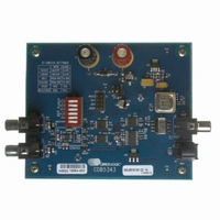
CDB5343
Manufacturer Part Number
CDB5343
Description
EvalBd 98dB 24-bit 96kHz Stereo ADC
Manufacturer
Cirrus Logic Inc
Specifications of CDB5343
Number Of Adc's
1
Number Of Bits
24
Sampling Rate (per Second)
108k
Data Interface
Serial
Inputs Per Adc
2 Single
Power (typ) @ Conditions
60mW @ 5 V
Voltage Supply Source
Single Supply
Operating Temperature
-40°C ~ 85°C
Utilized Ic / Part
CS5343, CS5344
Description/function
Audio A/D
Operating Supply Voltage
5 V
Product
Audio Modules
Lead Free Status / RoHS Status
Contains lead / RoHS non-compliant
For Use With/related Products
CS5343
Lead Free Status / RoHS Status
Contains lead / RoHS non-compliant, Contains lead / RoHS non-compliant
Other names
598-1156


16
4.4.1
4.5
Grounding and Power Supply Decoupling
As with any high-resolution converter, designing with the CS5343/4 requires careful attention to power sup-
ply and grounding arrangements if its potential performance is to be realized.
mended power arrangements, with VA connected to a clean supply. Decoupling capacitors should be as
near to the ADC as possible, with the low value ceramic capacitor being the nearest. All signals, especially
clocks, should be kept away from the FILT+ and VQ pins in order to avoid unwanted coupling into the mod-
ulators. The FILT+ and VQ decoupling capacitors, particularly the 0.1 µF, must be positioned to minimize
the electrical path from FILT+ to GND. The CDB5343 evaluation board demonstrates the optimum layout
and power supply arrangements. To minimize digital noise, connect the ADC digital outputs only to CMOS
inputs.
Component Values
Three parameters determine the values of resistors R1 and R2 as shown in
attenuation, and input impedance.
Figure 7
the discussion above, this circuit provides an optimal interface for both the ADC and the signal source.
First, consumer equipment frequently requires an input impedance of 10 kΩ, which the 4.99 kΩ resistors
provide. Second, this circuit will attenuate a typical line level voltage, 2 Vrms, to the full-scale input of the
ADC, 1 Vrms when VA = 5 V. Finally, at 2.5 kΩ, the source impedance optimizes analog performance of
the ADC.
•
•
•
Source Impedance: Source impedance is defined as the impedance as seen from the ADC looking
back into the signal network. The ADC achieves optimal THD+N performance with a source imped-
ance less than or equal to 2.5 kΩ.
Attenuation: The required attenuation factor depends on the magnitude of the input signal. The full-
scale input voltage is specified under
The user should select values for R1 and R2 such that the magnitude of the incoming signal multiplied
by the attenuation factor is less than or equal to the full-scale input voltage of the device.
Input Impedance: Input impedance is the impedance from the signal source to the ADC analog input
pins, including the ADC. Because the ADC’s input impedance (see the
mercial Grade
typically used for the input attenuator, its contribution can be neglected when calculating the input im-
pedance.
tenuator.
illustrates an example configuration using two 4.99 kΩ resistors in place of R1 and R2. Based on
Table 6
(-CZZ)” table on
Input
Figure 7. CS5343/4 Example Analog Input Network
shows the input parameters and the associated design equations for the input at-
Source Impedance
Attenuation Factor
Table 6. Analog Input Design Parameters
4.99 kΩ
4.99 kΩ
Input Impedance
Table 6
page
“Analog Characteristics - Commercial Grade (-CZZ)” on page
6) is several orders of magnitude larger than the resistor values
1 µF
180pF
C0G
shows the design equation used to determine these values.
4/2/08
Draft
(
------------------------ -
------------------------ -
(
(
R1 R2
R1
R1
R1
(
R2
×
+
+
+
CS5343/4
AIN
R2
R2
R2
)
)
)
)
“Analog Characteristics - Com-
Figure
Figure 3
6: source impedance,
shows the recom-
CS5343/4
DS687F3
6.
Related parts for CDB5343
Image
Part Number
Description
Manufacturer
Datasheet
Request
R

Part Number:
Description:
Development Kit
Manufacturer:
Cirrus Logic Inc
Datasheet:
Part Number:
Description:
Development Kit
Manufacturer:
Cirrus Logic Inc
Datasheet:


Part Number:
Description:
High-efficiency PFC + Fluorescent Lamp Driver Reference Design
Manufacturer:
Cirrus Logic Inc
Datasheet:
Part Number:
Description:
Development Kit
Manufacturer:
Cirrus Logic Inc
Datasheet:
Part Number:
Description:
Development Kit
Manufacturer:
Cirrus Logic Inc
Datasheet:

Part Number:
Description:
Development Kit
Manufacturer:
Cirrus Logic Inc
Datasheet:
Part Number:
Description:
Development Kit
Manufacturer:
Cirrus Logic Inc
Datasheet:
Part Number:
Description:
Development Kit
Manufacturer:
Cirrus Logic Inc
Datasheet:
Part Number:
Description:
Development Kit
Manufacturer:
Cirrus Logic Inc
Datasheet:

Part Number:
Description:
EVALUATION BOARD FOR CS8427
Manufacturer:
Cirrus Logic Inc
Datasheet:

Part Number:
Description:
BOARD EVAL FOR CS8416 RCVR
Manufacturer:
Cirrus Logic Inc
Datasheet:

Part Number:
Description:
EVALUATION BOARD FOR CS8420
Manufacturer:
Cirrus Logic Inc
Datasheet:

Part Number:
Description:
KIT DEVELOPMENT EP9315 ARM9
Manufacturer:
Cirrus Logic Inc
Datasheet:

Part Number:
Description:
KIT DEVELOPMENT EP9302 ARM9
Manufacturer:
Cirrus Logic Inc
Datasheet: