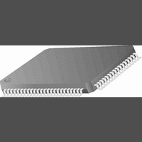
DS92LV18TVV National Semiconductor, DS92LV18TVV Datasheet - Page 19

DS92LV18TVV
Manufacturer Part Number
DS92LV18TVV
Description
Line Receiver IC
Manufacturer
National Semiconductor
Datasheet
1.DS92LV18TVV.pdf
(20 pages)
Specifications of DS92LV18TVV
Driver Case Style
LQFP
No. Of Pins
80
Peak Reflow Compatible (260 C)
No
Supply Voltage Max
3.3V
Leaded Process Compatible
No
Package / Case
80-LQFP
Lead Free Status / RoHS Status
Contains lead / RoHS non-compliant
Available stocks
Company
Part Number
Manufacturer
Quantity
Price
Company:
Part Number:
DS92LV18TVV/NOPB
Manufacturer:
TI
Quantity:
1 000
Company:
Part Number:
DS92LV18TVV/NOPB
Manufacturer:
TI
Quantity:
2 170
Company:
Part Number:
DS92LV18TVV/NOPB
Manufacturer:
Texas Instruments
Quantity:
10 000
Part Number:
DS92LV18TVV/NOPB
Manufacturer:
NS/国半
Quantity:
20 000
Company:
Part Number:
DS92LV18TVVX/NOPB
Manufacturer:
TI
Quantity:
1 000
Company:
Part Number:
DS92LV18TVVX/NOPB
Manufacturer:
Texas Instruments
Quantity:
10 000
3, 18,21, 22, 23, 24, 25,
Pin Descriptions
Note 10: Input defaults to "low" state when left open due to an internal on-chip pull-down circuit.
26, 27, 28, 33, 34, 35,
41, 44, 51, 52, 59, 60,
45, 46, 47, 48, 54, 55,
56, 57, 62, 64, 65, 66,
67, 70, 71, 72, 73, 80
36, 37, 38, 39, 40
43, 50, 53, 58, 69
Pin #
5, 10, 11, 15
6,9,12,16
61, 68
29,32
30,31
74,76
75,77
13
14
17
19
20
42
49
63
78
79
1
2
4
7
8
ROUT (0:17)
LOCAL_LE
Pin Name
DIN (0:17)
LINE_LE
REFCLK
RPWDN
TPWDN
AGND
PGND
DGND
PGND
AVDD
SYNC
PVDD
DVDD
PVDD
RCLK
LOCK
TCLK
RIN+
REN
RIN-
DO+
DEN
DO-
CMOS, O Receiver Outputs.
CMOS, O Recovered Clock. Parallel data rate clock recovered from
CMOS, O LOCK indicates the status of the receiver PLL. LOCK = H -
LVDS, O Transmitter LVDS True Output
LVDS, O Transmitter LVDS Inverting Output
CMOS, I
CMOS, I
CMOS, I
CMOS, I
CMOS, I
CMOS, I
CMOS, I
CMOS, I
CMOS, I
CMOS, I
LVDS, I
LVDS, I
I/O
RPWDN = Low will put the Receiver in low power, stand-by, mode.
Note: The Receiver PLL will lose lock.(Note 10)
REN = Low will disable the Receiver outputs. Receiver PLL
remains locked. (See LOCK pin description)(Note 10)
Frequency reference clock input for the receiver.
Analog Voltage Supply
Analog Ground
Receiver LVDS True Input
Receiver LVDS Inverting Input
Transmitter reference clock. Used to strobe data at the DIN Inputs
and to drive the transmitter PLL. See TCLK Timing Requirements.
DEN = Low will disable the Transmitter outputs. The transmitter
PLL will remain locked.(Note 10)
SYNC = High will cause the transmitter to ignore the data inputs
and send SYNC patterns to provide a locking reference to
receiver(s). See Functional Description.(Note 10)
Transmitter data inputs.(Note 10)
PLL Ground.
PLL Voltage supply.
Digital Ground.
TPWDN = Low will put the Transmitter in low power, stand-by
mode. Note: The transmitter PLL will lose lock.(Note 10)
Digital Voltage Supplies.
embedded clock. Used to strobe ROUT (0:17). LVCMOS Level
output.
receiver PLL is unlocked, LOCK = L - receiver PLL is locked.
PLL Grounds.
PLL Voltage Supplies.
LINE_LE = High enables the receiver loopback mode. Data
received at the RIN
outputs.(Note 10)
LOCAL_LE = High enables the transmitter loopback mode. Data
received at the DIN inputs is fed back through the ROUT
outputs.(Note 10)
19
±
inputs is fed back through the DO
Description
www.national.com
±


