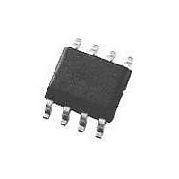
LMH6715MA National Semiconductor, LMH6715MA Datasheet - Page 10

LMH6715MA
Manufacturer Part Number
LMH6715MA
Description
Operational Amplifier (Op-Amp) IC
Manufacturer
National Semiconductor
Datasheet
1.LMH6715MA.pdf
(12 pages)
Specifications of LMH6715MA
Bandwidth
480MHz
Slew Rate
1300V/µs
No. Of Pins
8
Peak Reflow Compatible (260 C)
No
Input Offset Voltage Max
8mV
Leaded Process Compatible
No
Mounting Type
Surface Mount
Package / Case
8-SOIC
Number Of Channels
2
Voltage Gain Db
60 dB
Common Mode Rejection Ratio (min)
50 dB
Input Offset Voltage
6 mV at +/- 5 V
Supply Current
15.2 mA at +/- 5 V
Maximum Operating Temperature
+ 85 C
Maximum Dual Supply Voltage
+/- 6 V
Minimum Operating Temperature
- 40 C
Lead Free Status / RoHS Status
Contains lead / RoHS non-compliant
Available stocks
Company
Part Number
Manufacturer
Quantity
Price
Part Number:
LMH6715MA
Manufacturer:
NS/国半
Quantity:
20 000
Part Number:
LMH6715MAX
Manufacturer:
NS/国半
Quantity:
20 000
www.national.com
Application Introduction
has a typical short term settling time to 0.05% of 12ns for a
2V step. Also, the amplifier is virtually free of any long term
thermal tail effects at low gains.
When measuring settling time, a solid ground plane should
be used in order to reduce ground inductance which can
cause common-ground-impedance coupling. Power supply
and ground trace parasitic capacitances and the load ca-
pacitance will also affect settling time.
Placing a series resistor (R
mended for optimal settling time performance when driving a
capacitive load. The Typical Performance plot labeled “R
and Settling Time vs. Capacitive Load” provides a means for
selecting a value of R
DC & NOISE PERFORMANCE
A current-feedback amplifier’s input stage does not have
equal nor correlated bias currents, therefore they cannot be
canceled and each contributes to the total DC offset voltage
at the output by the following equation:
The input resistance is the resistance looking from the non-
inverting input back toward the source. For inverting DC-
offset calculations, the source resistance seen by the input
resistor R
as a part of the non-inverting gain equation. Application note
OA-7 gives several circuits for DC offset correction. The
noise currents for the inverting and non-inverting inputs are
graphed in the Typical Performance plot labeled “Equivalent
Input Noise”. A more complete discussion of amplifier input-
referred noise and external resistor noise contribution can be
found in OA-12.
DIFFERENTIAL GAIN & PHASE
The LMH6715 can drive multiple video loads with very low
differential gain and phase errors. The Typical Performance
plots labeled “Differential Gain vs. Frequency” and “Differen-
tial Phase vs. Frequency” show performance for loads from
1 to 4. The Electrical Characteristics table also specifies
performance for one 150Ω load at 4.43MHz. For NTSC
video, the performance specifications also apply. Application
note OA-24 “Measuring and Improving Differential Gain &
Differential Phase for Video”, describes in detail the tech-
niques used to measure differential gain and phase.
I/O VOLTAGE & OUTPUT CURRENT
The usable common-mode input voltage range (CMIR) of
the LMH6715 specified in the Electrical Characteristics table
of the data sheet shows a range of
this range will cause the input stage to saturate and clip the
output signal.
The output voltage range is determined by the load resistor
and the choice of power supplies. With
output driver will typically drive
of 100Ω. Increasing the supply voltages will change the
common-mode input and output voltage swings while at the
same time increase the internal junction temperature.
g
must be included in the output offset calculation
s
for a given capacitive load.
s
) at the output pin is recom-
±
3.9V into a load resistance
±
±
2.2 volts. Exceeding
5 volts the class A/B
(Continued)
S
10
Applications Circuits
SINGLE-TO-DIFFERENTIAL LINE DRIVER
The LMH6715’s well matched AC channel-response allows a
single-ended input to be transformed to highly matched
push-pull driver. From a 1V single-ended input the circuit of
Figure 3 produces 1V differential signal between the two
outputs. For larger signals the input voltage divider (R
2R
DIFFERENTIAL LINE RECEIVER
Figure 4 and Figure 5 show two different implementations of
an instrumentation amplifier which convert differential sig-
nals to single-ended. Figure 5 allows CMRR adjustment
through R
2
) is necessary to limit the input voltage on channel 2.
FIGURE 3. Single-to-Differential Line Driver
2
FIGURE 4. Differential Line Receiver
.
20042945
20042946
1
=


