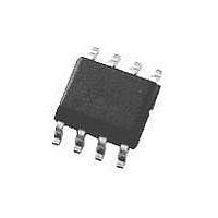
LMH6715MA National Semiconductor, LMH6715MA Datasheet - Page 8

LMH6715MA
Manufacturer Part Number
LMH6715MA
Description
Operational Amplifier (Op-Amp) IC
Manufacturer
National Semiconductor
Datasheet
1.LMH6715MA.pdf
(12 pages)
Specifications of LMH6715MA
Bandwidth
480MHz
Slew Rate
1300V/µs
No. Of Pins
8
Peak Reflow Compatible (260 C)
No
Input Offset Voltage Max
8mV
Leaded Process Compatible
No
Mounting Type
Surface Mount
Package / Case
8-SOIC
Number Of Channels
2
Voltage Gain Db
60 dB
Common Mode Rejection Ratio (min)
50 dB
Input Offset Voltage
6 mV at +/- 5 V
Supply Current
15.2 mA at +/- 5 V
Maximum Operating Temperature
+ 85 C
Maximum Dual Supply Voltage
+/- 6 V
Minimum Operating Temperature
- 40 C
Lead Free Status / RoHS Status
Contains lead / RoHS non-compliant
Available stocks
Company
Part Number
Manufacturer
Quantity
Price
Part Number:
LMH6715MA
Manufacturer:
NS/国半
Quantity:
20 000
Part Number:
LMH6715MAX
Manufacturer:
NS/国半
Quantity:
20 000
www.national.com
Application Section
Application Introduction
Offered in an 8-pin package for reduced space and cost, the
wideband LMH6715 dual current-feedback op amp provides
closely matched DC and AC electrical performance charac-
teristics making the part an ideal choice for wideband signal
processing. Applications such as broadcast quality video
systems, IQ amplifiers, filter blocks, high speed peak detec-
tors, integrators and transimedance amplifiers will all find
superior performance in the LMH6715 dual op amp.
FIGURE 2. Inverting Configuration with Power Supply
FIGURE 1. Non-Inverting Configuration with Power
Supply Bypassing
Bypassing
20042935
20042937
8
FEEDBACK RESISTOR SELECTION
One of the key benefits of a current feedback operational
amplifier is the ability to maintain optimum frequency re-
sponse independent of gain by using appropriate values for
the feedback resistor (R
Typical Performance plots specify an R
+2V/V and
Generally, lowering R
peak the frequency response and extend the bandwidth
while increasing the value of R
response to roll off faster. Reducing the value of R
below it’s recommended value will cause overshoot, ringing
and, eventually, oscillation.
The plot labeled “Frequency Response vs. R
LMH6715’s frequency response as R
A
peaking and marginal stability. An R
maximal bandwidth and gain flatness with good stability, but
with very light loads (R
peaking. An R
bandwidth and is the recommended value for most applica-
tions. Since all applications are slightly different it is worth
some experimentation to find the optimal R
circuit. For more information see Application Note OA-13
which describes the relationship between R
loop frequency response for current feedback operational
amplifiers.
When configuring the LMH6715 for gains other than +2V/V,
it is usually necessary to adjust the value of the feedback
resistor. The two plots labeled “R
and “R
resistor values for a number of gain selections.
V
= +2). This plot shows that an R
F
vs. Inverting Gain” provide recommended feedback
±
5V power supplies (unless otherwise specified).
F
Frequency Response vs. R
of 500Ω gives excellent stability with good
L
F
F
>
). The Electrical Characteristics and
from it’s recommended value will
300Ω) the device may show some
F
F
will cause the frequency
vs. Non-inverting Gain”
F
F
is varied (R
F
F
of 300Ω gives near
of 200Ω results in
of 500Ω, a gain of
F
F
F
F
” shows the
and closed-
for a given
20042914
L
F
= 100Ω,
too far


