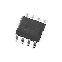
LMH6715MA National Semiconductor, LMH6715MA Datasheet - Page 2

LMH6715MA
Manufacturer Part Number
LMH6715MA
Description
Operational Amplifier (Op-Amp) IC
Manufacturer
National Semiconductor
Datasheet
1.LMH6715MA.pdf
(12 pages)
Specifications of LMH6715MA
Bandwidth
480MHz
Slew Rate
1300V/µs
No. Of Pins
8
Peak Reflow Compatible (260 C)
No
Input Offset Voltage Max
8mV
Leaded Process Compatible
No
Mounting Type
Surface Mount
Package / Case
8-SOIC
Number Of Channels
2
Voltage Gain Db
60 dB
Common Mode Rejection Ratio (min)
50 dB
Input Offset Voltage
6 mV at +/- 5 V
Supply Current
15.2 mA at +/- 5 V
Maximum Operating Temperature
+ 85 C
Maximum Dual Supply Voltage
+/- 6 V
Minimum Operating Temperature
- 40 C
Lead Free Status / RoHS Status
Contains lead / RoHS non-compliant
Available stocks
Company
Part Number
Manufacturer
Quantity
Price
Part Number:
LMH6715MA
Manufacturer:
NS/国半
Quantity:
20 000
Part Number:
LMH6715MAX
Manufacturer:
NS/国半
Quantity:
20 000
www.national.com
Frequency Domain Response
SSBW
LSBW
GFP
GFR
LPD
DG
DP
Time Domain Response
Tr
Ts
OS
SR
Distortion And Noise Response
HD2
HD3
V
I
I
SNF
XTLKA
Static, DC Performance
V
DV
I
DI
I
DI
PSRR
N
NN
BN
BI
Symbol
N
IO
Absolute Maximum Ratings
If Military/Aerospace specified devices are required,
please contact the National Semiconductor Sales Office/
Distributors for availability and specifications.
Electrical Characteristics
A
BN
BI
ESD Tolerance (Note 4)
V
I
Common-Mode Input Voltage
Differential Input Voltage
Maximum Junction Temperature
IO
OUT
V
CC
Human Body Model
Machine Model
= +2, R
-3dB Bandwidth
-3dB Bandwidth
Gain Flatness
Linear Phase Deviation
Differential Gain
Differential Phase
Rise and Fall Time
Settling Time to 0.05%
Overshoot
Slew Rate
2nd Harmonic Distortion
3rd Harmonic Distortion
Equivalent Input Noise
Crosstalk
Input Offset Voltage
Input Bias Current
Input Bias Current
Power Supply Rejection Ratio
F
Peaking
Rolloff
Non-Inverting Voltage
Inverting Current
Non-Inverting Current
Noise Floor
Average Drift
Average Drift
Average Drift
= 500Ω, V
Parameter
CC
=
±
5 V, R
L
= 100Ω; unless otherwise specified. Boldface limits apply at the temperature extremes.
V
V
V
DC to 100MHz, R
DC to 100MHz, R
DC to 100MHz, R
R
R
0.5V Step
4V Step
2V Step
0.5V Step
2V Step
2V
2V
>
>
>
>
Input Referred 10MHz
Non-Inverting
Inverting
DC
OUT
OUT
OUT
(Note 1)
L
L
1MHz
1MHz
1MHz
1MHz
PP
PP
= 150Ω, 4.43MHz
= 150Ω, 4.43MHz
(Note 3)
±
+150˚C
, 20MHz
, 20MHz
2000V
<
<
<
6.75V
±
150V
2.2V
V
0.5V
4.0V
0.5V
CC
Conditions
PP
PP
PP
, R
, R
2
F
F
F
F
F
= 300Ω
= 300Ω
= 300Ω
= 300Ω
= 300Ω
Operating Ratings
Storage Temperature Range
Lead Temperature (Soldering 10
sec)
Thermal Resistance
Operating Temperature Range
Nominal Operating Voltage
Package
SOIC
Min
280
46
44
65˚C/W
(θ
−153
1300
JC
0.25
0.02
0.02
10.0
Typ
−60
−75
−70
±
±
±
400
170
0.1
0.1
1.4
3.4
1.4
±
±
±
12
60
3
1
30
30
20
)
2
5
6
−65˚C to +150˚C
Max
±
±
±
±
±
±
12
20
21
35
−40˚C to +85˚C
6
8
145˚C/W
(θ
±
5V to
JA
+300˚C
nV/
pA/
pA/
)
dB
µV/˚C
nA/˚C
nA/˚C
Units
MHz
MHz
V/µs
dBc
dBc
deg
deg
mV
dB
dB
dB
µA
µA
dB
ns
ns
ns
%
%
±
1Hz
6V


