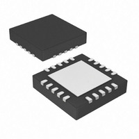
PIC16F785T-I/ML Microchip Technology, PIC16F785T-I/ML Datasheet - Page 48

PIC16F785T-I/ML
Manufacturer Part Number
PIC16F785T-I/ML
Description
3.5 KB Flash, 128 RAM, 18 I/O 20 QFN 4x4mm T/R
Manufacturer
Microchip Technology
Series
PIC® 16Fr
Datasheets
1.PIC16F616T-ISL.pdf
(8 pages)
2.PIC16F785-ISS.pdf
(206 pages)
3.PIC16F785-ISS.pdf
(10 pages)
4.PIC16F785-ISS.pdf
(28 pages)
Specifications of PIC16F785T-I/ML
Core Processor
PIC
Core Size
8-Bit
Speed
20MHz
Peripherals
Brown-out Detect/Reset, POR, PWM, WDT
Number Of I /o
17
Program Memory Size
3.5KB (2K x 14)
Program Memory Type
FLASH
Eeprom Size
256 x 8
Ram Size
128 x 8
Voltage - Supply (vcc/vdd)
2 V ~ 5.5 V
Data Converters
A/D 14x10b
Oscillator Type
Internal
Operating Temperature
-40°C ~ 85°C
Package / Case
20-VQFN Exposed Pad, 20-HVQFN, 20-SQFN, 20-DHVQFN
Lead Free Status / RoHS Status
Lead free / RoHS Compliant
Connectivity
-
Lead Free Status / RoHS Status
Lead free / RoHS Compliant, Lead free / RoHS Compliant
- PIC16F616T-ISL PDF datasheet
- PIC16F785-ISS PDF datasheet #2
- PIC16F785-ISS PDF datasheet #3
- PIC16F785-ISS PDF datasheet #4
- Current page: 48 of 206
- Download datasheet (4Mb)
PIC16F785/HV785
4.4.1
Each PORTC pin is multiplexed with other functions.
The pins and their combined functions are briefly
described here. For specific information about individ-
ual functions such as the comparator or the A/D, refer
to the appropriate section in this Data Sheet.
4.4.1.1
The RC0 is configurable to function as one of the
following:
• General purpose I/O
• Analog input for the A/D Converter
• Non-inverting input to Comparator 2
4.4.1.2
The RC6/AN8/OP1- pin is configurable to function as
one of the following:
• General purpose I/O
• Analog input for the A/D
• Inverting input for Op Amp 1
4.4.1.3
The RC7/AN9/OP1+ pin is configurable to function as
one of the following:
• General purpose I/O
• Analog input for the A/D
• Non-inverting input for Op Amp 1
FIGURE 4-10:
DS41249E-page 46
PORTC
TRISC
TRISC
Data Bus
PORTC
WR
WR
RD
RD
D
D
To Op Amp1 (RC6, RC7)
To Comparators (RC0)
To A/D Converter
CK
CK
PORTC PIN DESCRIPTIONS AND
DIAGRAMS
RC0/AN4/C2IN+
RC6/AN8/OP1-
RC7/AN9/OP1+
Q
Q
Q
Q
BLOCK DIAGRAM OF
RC0, RC6 AND RC7
Q
ANS4 (RC0)
ANS8 (RC6)
ANS9 (RC7)
EN
D
V
V
DD
SS
I/O Pin
4.4.1.4
The RC1 is configurable to function as one of the
following:
• General purpose I/O
• Analog input for the A/D Converter
• Analog input to Comparators 1 and 2
• Digital output from the Two-Phase PWM
FIGURE 4-11:
PORTC
PORTC
TRISC
TRISC
Data Bus
PH1EN
PH1
WR
WR
RD
RD
To Comparators
To A/D Converter
D
D
CK
CK
RC1/AN5/C12IN1-/PH1
Q
Q
Q
Q
BLOCK DIAGRAM OF RC1
Q
© 2008 Microchip Technology Inc.
EN
D
1
0
ANS5
V
V
DD
SS
I/O Pin
Related parts for PIC16F785T-I/ML
Image
Part Number
Description
Manufacturer
Datasheet
Request
R

Part Number:
Description:
IC PIC MCU FLASH 2KX14 20SOIC
Manufacturer:
Microchip Technology
Datasheet:

Part Number:
Description:
IC PIC MCU FLASH 2KX14 20QFN
Manufacturer:
Microchip Technology
Datasheet:

Part Number:
Description:
IC PIC MCU FLASH 2KX14 20DIP
Manufacturer:
Microchip Technology
Datasheet:

Part Number:
Description:
IC PIC MCU FLASH 2KX14 20SSOP
Manufacturer:
Microchip Technology
Datasheet:

Part Number:
Description:
IC PIC MCU FLASH 2KX14 20SOIC
Manufacturer:
Microchip Technology
Datasheet:

Part Number:
Description:
IC PIC MCU FLASH 2KX14 20DIP
Manufacturer:
Microchip Technology
Datasheet:

Part Number:
Description:
3.5 KB Flash, 128 RAM, 18 I/O 20 QFN 4x4mm TUBE
Manufacturer:
Microchip Technology
Datasheet:

Part Number:
Description:
20 PIN, 3.5 KB STD FLASH, 128 RAM, 18 I/O PB FREE,
Manufacturer:
Microchip Technology
Datasheet:

Part Number:
Description:
IC, 8BIT MCU, PIC16F, 32MHZ, SOIC-18
Manufacturer:
Microchip Technology
Datasheet:

Part Number:
Description:
IC, 8BIT MCU, PIC16F, 32MHZ, SSOP-20
Manufacturer:
Microchip Technology
Datasheet:

Part Number:
Description:
IC, 8BIT MCU, PIC16F, 32MHZ, DIP-18
Manufacturer:
Microchip Technology
Datasheet:

Part Number:
Description:
IC, 8BIT MCU, PIC16F, 32MHZ, QFN-28
Manufacturer:
Microchip Technology
Datasheet:

Part Number:
Description:
IC, 8BIT MCU, PIC16F, 32MHZ, QFN-28
Manufacturer:
Microchip Technology
Datasheet:

Part Number:
Description:
IC, 8BIT MCU, PIC16F, 32MHZ, QFN-28
Manufacturer:
Microchip Technology
Datasheet:

Part Number:
Description:
IC, 8BIT MCU, PIC16F, 32MHZ, SSOP-20
Manufacturer:
Microchip Technology
Datasheet:


