PIC16HV785-E/P Microchip Technology, PIC16HV785-E/P Datasheet - Page 45
PIC16HV785-E/P
Manufacturer Part Number
PIC16HV785-E/P
Description
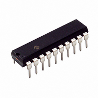
3.5KB Flash, 128 RAM, 18 I/O 20 PDIP .300in TUBE
Manufacturer
Microchip Technology
Series
PIC® 16Fr
Datasheets
1.PIC16F616T-ISL.pdf
(8 pages)
2.PIC16F785-ISS.pdf
(206 pages)
3.PIC16F785-ISS.pdf
(10 pages)
4.PIC16F785-ISS.pdf
(28 pages)
Specifications of PIC16HV785-E/P
Core Processor
PIC
Core Size
8-Bit
Speed
20MHz
Peripherals
Brown-out Detect/Reset, POR, PWM, WDT
Number Of I /o
17
Program Memory Size
3.5KB (2K x 14)
Program Memory Type
FLASH
Eeprom Size
256 x 8
Ram Size
128 x 8
Voltage - Supply (vcc/vdd)
2 V ~ 5.5 V
Data Converters
A/D 14x10b
Oscillator Type
Internal
Operating Temperature
-40°C ~ 125°C
Package / Case
20-DIP (0.300", 7.62mm)
Processor Series
PIC16H
Core
PIC
Data Bus Width
8 bit
Data Ram Size
128 B
Interface Type
RS- 232, USB
Maximum Clock Frequency
32 MHz
Number Of Programmable I/os
18
Number Of Timers
3
Maximum Operating Temperature
+ 125 C
Mounting Style
Through Hole
3rd Party Development Tools
52715-96, 52716-328, 52717-734
Development Tools By Supplier
PG164130, DV164035, DV244005, DV164005, PG164120, ICE2000, DV164120, DM163029
Minimum Operating Temperature
- 40 C
On-chip Adc
10 bit, 14 Channel
Lead Free Status / RoHS Status
Lead free / RoHS Compliant
For Use With
AC162060 - HEADER INTRFC MPLAB ICD2 20PINAC164039 - MODULE SKT PROMATE II 20DIP/SOICACICE0203 - MPLABICE 20P 300 MIL ADAPTER
Connectivity
-
Lead Free Status / Rohs Status
Details
Available stocks
Company
Part Number
Manufacturer
Quantity
Price
Company:

Part Number:
PIC16HV785-E/P
Manufacturer:
MICROCHIP
Quantity:
12 000


4.3.1
Each PORTB pin is multiplexed with other functions.
The pins and their combined functions are briefly
described here. For specific information about individ-
ual functions such as the PWM, operational amplifier,
or the A/D, refer to the appropriate section in this Data
Sheet.
4.3.1.1
The RB4/AN10/OP2- pin is configurable to function as
one of the following:
• General purpose I/O
• Analog input to the A/D
• Analog input to Op Amp 2
4.3.1.2
The RB5/AN11/OP2+ pin is configurable to function as
one of the following:
• General purpose I/O
• Analog input to the A/D
• Analog input to Op Amp 2
FIGURE 4-7:
© 2008 Microchip Technology Inc.
PORTB
PORTB
Data Bus
TRISB
TRISB
WR
WR
RD
RD
D
D
To Op Amp 2
To A/D Converter
CK
CK
PORTB PIN DESCRIPTIONS AND
DIAGRAMS
RB4/AN10/OP2-
RB5/AN11/OP2+
Q
Q
Q
Q
BLOCK DIAGRAM OF RB4
AND RB5
Q
ANS10 (RB4)
ANS11 (RB5)
EN
D
V
V
DD
SS
I/O Pin
4.3.1.3
The RB6 pin is configurable to function as the following:
• Open drain general purpose I/O
FIGURE 4-8:
4.3.1.4
The RB7/SYNC pin is configurable to function as one
of the following:
• General purpose I/O
• PWM synchronization input and output
FIGURE 4-9:
PORTB
PORTB
PORTB
PORTB
TRISB
TRISB
TRISB
TRISB
Data Bus
PH1EN
PH2EN
PWM Master
Sync out
Data Bus
WR
WR
RD
WR
WR
RD
RD
RD
to PWM Sync Input
PIC16F785/HV785
D
D
D
D
CK
CK
CK
CK
RB6
RB7/SYNC
Q
Q
Q
Q
Q
Q
Q
Q
BLOCK DIAGRAM OF RB6
BLOCK DIAGRAM OF RB7
Q
Q
EN
EN
D
D
1
0
DS41249E-page 43
N
V
SS
V
V
V
SS
DD
SS
I/O Pin
I/O Pin
Related parts for PIC16HV785-E/P
Image
Part Number
Description
Manufacturer
Datasheet
Request
R

Part Number:
Description:
Manufacturer:
Microchip Technology Inc.
Datasheet:
Part Number:
Description:
Manufacturer:
Microchip Technology Inc.
Datasheet:
Part Number:
Description:
Manufacturer:
Microchip Technology Inc.
Datasheet:
Part Number:
Description:
Manufacturer:
Microchip Technology Inc.
Datasheet:
Part Number:
Description:
Manufacturer:
Microchip Technology Inc.
Datasheet:
Part Number:
Description:
Manufacturer:
Microchip Technology Inc.
Datasheet:
Part Number:
Description:
Manufacturer:
Microchip Technology Inc.
Datasheet:
Part Number:
Description:
Manufacturer:
Microchip Technology Inc.
Datasheet: