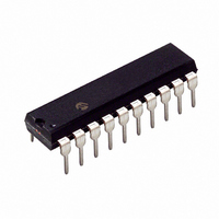
PIC16HV785-E/P Microchip Technology, PIC16HV785-E/P Datasheet - Page 79

PIC16HV785-E/P
Manufacturer Part Number
PIC16HV785-E/P
Description
3.5KB Flash, 128 RAM, 18 I/O 20 PDIP .300in TUBE
Manufacturer
Microchip Technology
Series
PIC® 16Fr
Datasheets
1.PIC16F616T-ISL.pdf
(8 pages)
2.PIC16F785-ISS.pdf
(206 pages)
3.PIC16F785-ISS.pdf
(10 pages)
4.PIC16F785-ISS.pdf
(28 pages)
Specifications of PIC16HV785-E/P
Core Processor
PIC
Core Size
8-Bit
Speed
20MHz
Peripherals
Brown-out Detect/Reset, POR, PWM, WDT
Number Of I /o
17
Program Memory Size
3.5KB (2K x 14)
Program Memory Type
FLASH
Eeprom Size
256 x 8
Ram Size
128 x 8
Voltage - Supply (vcc/vdd)
2 V ~ 5.5 V
Data Converters
A/D 14x10b
Oscillator Type
Internal
Operating Temperature
-40°C ~ 125°C
Package / Case
20-DIP (0.300", 7.62mm)
Processor Series
PIC16H
Core
PIC
Data Bus Width
8 bit
Data Ram Size
128 B
Interface Type
RS- 232, USB
Maximum Clock Frequency
32 MHz
Number Of Programmable I/os
18
Number Of Timers
3
Maximum Operating Temperature
+ 125 C
Mounting Style
Through Hole
3rd Party Development Tools
52715-96, 52716-328, 52717-734
Development Tools By Supplier
PG164130, DV164035, DV244005, DV164005, PG164120, ICE2000, DV164120, DM163029
Minimum Operating Temperature
- 40 C
On-chip Adc
10 bit, 14 Channel
Lead Free Status / RoHS Status
Lead free / RoHS Compliant
For Use With
AC162060 - HEADER INTRFC MPLAB ICD2 20PINAC164039 - MODULE SKT PROMATE II 20DIP/SOICACICE0203 - MPLABICE 20P 300 MIL ADAPTER
Connectivity
-
Lead Free Status / Rohs Status
Details
Available stocks
Company
Part Number
Manufacturer
Quantity
Price
Company:
Part Number:
PIC16HV785-E/P
Manufacturer:
MICROCHIP
Quantity:
12 000
11.3
A device Reset forces all registers to their Reset state.
This disables both op amps.
11.4
Common AC and DC performance specifications for
the OPA module:
• Common Mode Voltage Range
• Leakage Current
• Input Offset Voltage
• Open Loop Gain
• Gain Bandwidth Product (GBWP)
Common mode voltage range is the specified voltage
range for the OPA+ and OPA- inputs, for which the OPA
module will perform to within its specifications. The
OPA module is designed to operate with input voltages
between 0 and V
voltages greater than V
beyond the normal operating range.
TABLE 11-1:
© 2008 Microchip Technology Inc.
Name
ANSEL0
ANSEL1
OPA1CON
OPA2CON
TRISB
TRISC
Legend:
Effects of a Reset
OPA Module Performance
x = unknown, u = unchanged, - = unimplemented, read as ‘0’. Shaded cells are not used for the OPA module.
OPAON
OPAON
TRISB7 TRISB6
TRISC7 TRISC6
ANS7
Bit 7
—
DD
REGISTERS ASSOCIATED WITH THE OPA MODULE
-1.4V. Behavior for common mode
ANS6
Bit 6
—
—
—
DD
-1.4V, or below 0V, are
TRISC5
TRISB5
ANS5
Bit 5
—
—
—
TRISB4
TRISC4
ANS4
Bit 4
—
—
—
TRISC3
ANS11
ANS3
Bit 3
—
—
—
TRISC2
ANS10
ANS2
Leakage current is a measure of the small source or
sink currents on the OPA+ and OPA- inputs. To mini-
mize the effect of leakage currents, the effective imped-
ances connected to the OPA+ and OPA- inputs should
be kept as small as possible and equal.
Input offset voltage is a measure of the voltage differ-
ence between the OPA+ and OPA- inputs in a closed
loop circuit with the OPA in its linear region. The offset
voltage will appear as a DC offset in the output equal to
the input offset voltage, multiplied by the gain of the
circuit. The input offset voltage is also affected by the
common mode voltage.
Open loop gain is the ratio of the output voltage to the
differential input voltage, (OPA+) - (OPA-). The gain is
greatest at DC and falls off with frequency.
Gain Bandwidth Product or GBWP is the frequency
at which the open loop gain falls off to 0 dB.
11.5
When enabled, the op amps continue to operate and
consume current while the processor is in Sleep mode.
Bit 2
—
—
—
PIC16F785/HV785
TRISC1
Effects of Sleep
ANS1
ANS9
Bit 1
—
—
—
TRISC0
ANS0
ANS8
Bit 0
—
—
—
1111 1111
---- 1111
0--- ----
0--- ----
1111 ----
1111 1111
POR, BOR
Value on
DS41249E-page 77
other Resets
Value on all
1111 1111
---- 1111
0--- ----
0--- ----
1111 ----
1111 1111


