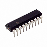
PIC16HV785-E/P Microchip Technology, PIC16HV785-E/P Datasheet - Page 61

PIC16HV785-E/P
Manufacturer Part Number
PIC16HV785-E/P
Description
3.5KB Flash, 128 RAM, 18 I/O 20 PDIP .300in TUBE
Manufacturer
Microchip Technology
Series
PIC® 16Fr
Datasheets
1.PIC16F616T-ISL.pdf
(8 pages)
2.PIC16F785-ISS.pdf
(206 pages)
3.PIC16F785-ISS.pdf
(10 pages)
4.PIC16F785-ISS.pdf
(28 pages)
Specifications of PIC16HV785-E/P
Core Processor
PIC
Core Size
8-Bit
Speed
20MHz
Peripherals
Brown-out Detect/Reset, POR, PWM, WDT
Number Of I /o
17
Program Memory Size
3.5KB (2K x 14)
Program Memory Type
FLASH
Eeprom Size
256 x 8
Ram Size
128 x 8
Voltage - Supply (vcc/vdd)
2 V ~ 5.5 V
Data Converters
A/D 14x10b
Oscillator Type
Internal
Operating Temperature
-40°C ~ 125°C
Package / Case
20-DIP (0.300", 7.62mm)
Processor Series
PIC16H
Core
PIC
Data Bus Width
8 bit
Data Ram Size
128 B
Interface Type
RS- 232, USB
Maximum Clock Frequency
32 MHz
Number Of Programmable I/os
18
Number Of Timers
3
Maximum Operating Temperature
+ 125 C
Mounting Style
Through Hole
3rd Party Development Tools
52715-96, 52716-328, 52717-734
Development Tools By Supplier
PG164130, DV164035, DV244005, DV164005, PG164120, ICE2000, DV164120, DM163029
Minimum Operating Temperature
- 40 C
On-chip Adc
10 bit, 14 Channel
Lead Free Status / RoHS Status
Lead free / RoHS Compliant
For Use With
AC162060 - HEADER INTRFC MPLAB ICD2 20PINAC164039 - MODULE SKT PROMATE II 20DIP/SOICACICE0203 - MPLABICE 20P 300 MIL ADAPTER
Connectivity
-
Lead Free Status / Rohs Status
Details
Available stocks
Company
Part Number
Manufacturer
Quantity
Price
Company:
Part Number:
PIC16HV785-E/P
Manufacturer:
MICROCHIP
Quantity:
12 000
8.2.1
The user must configure the RC5/CCP1 pin as an
output by clearing the TRISC<5> bit.
8.2.2
Timer1 must be running in Timer mode or Synchro-
nized Counter mode if the CCP module is using the
compare feature. In Asynchronous Counter mode, the
compare operation may not work.
8.2.3
When Generate Software Interrupt mode is chosen
(CCP1M<3:0> = 1010), the RC5/CCP1 pin is not
affected. The CCP1IF bit of the PIR1 Register is set,
causing a CCP interrupt (if enabled). See Register 8-1.
TABLE 8-2:
© 2008 Microchip Technology Inc.
Name
CCP1CON
CCPR1L
CCPR1H
CM2CON1
INTCON
PIE1
PIR1
T1CON
TMR1L
TMR1H
TRISC
Legend:
Note:
module.
CCP1 PIN CONFIGURATION
Clearing the CCP1CON register will force
the RC5/CCP1 compare output latch to
the default low level. This is not the
PORTC I/O data latch.
TIMER1 MODE SELECTION
SOFTWARE INTERRUPT MODE
– = Unimplemented locations, read as ‘0’, u = unchanged, x = unknown. Shaded cells are not used by the Capture, Compare or Timer1
Capture/Compare/PWM Register 1 Low Byte
Capture/Compare/PWM Register 1 High Byte
MC1OUT MC2OUT
Holding Register for the Least Significant Byte of the 16-bit TMR1 Register
Holding Register for the Most Significant Byte of the 16-bit TMR1 Register
T1GINV
TRISC7
EEIE
Bit 7
EEIF
GIE
—
REGISTERS ASSOCIATED WITH CAPTURE, COMPARE, AND TIMER1
TMR1GE T1CKPS1
TRISC6
ADIE
Bit 6
PEIE
ADIF
—
CCP1IE
CCP1IF
TRISC5
DC1B1
Bit 5
T0IE
—
T1CKPS0
TRISC4
DC1B0
INTE
C2IE
Bit 4
C2IF
—
T1OSCEN
CCP1M3
TRISC3
RAIE
Bit 3
C1IE
C1IF
—
CCP1M2
T1SYNC
TRISC2
OSFIE
8.2.4
In this mode (CCP1M<3:0> = 1011), an internal
hardware trigger is generated, which may be used to
initiate an action. See Register 8-1.
The special event trigger output of the CCP occurs
immediately upon a match between the TMR1H,
TMR1L register pair and CCPR1H, CCPR1L register
pair. The TMR1H, TMR1L register pair is not reset until
the next rising edge of the TMR1 clock. This allows the
CCPR1H, CCPR1L register pair to effectively provide a
16-bit programmable period register for Timer1. The
special event trigger output also starts an A/D
conversion provided that the A/D module is enabled.
OSFIF
Bit 2
T0IF
—
Note 1: The special event trigger from the CCP
PIC16F785/HV785
CCP1M1
TMR1CS
2: Removing the match condition by chang-
TMR2IE
TMR2IF
TRISC1
T1GSS
Bit 1
INTF
SPECIAL EVENT TRIGGER
module will not set interrupt flag bit
TMR1IF (PIR1<0>).
ing the contents of the CCPR1H and
CCPR1L register pair between the clock
edge that generates the special event
trigger and the clock edge that generates
the TMR1 Reset, will preclude the Reset
from occurring.
TMR1ON
CCP1M0
C2SYNC
TMR1IE
TMR1IF
TRISC0
RAIF
Bit 0
--00 0000
xxxx xxxx
xxxx xxxx
00-- --10
0000 0000
0000 0000
0000 0000
0000 0000
xxxx xxxx
xxxx xxxx
--11 1111
POR, BOR
Value on
DS41249E-page 59
other Resets
Value on all
--00 0000
uuuu uuuu
uuuu uuuu
00-- --10
0000 0000
0000 0000
0000 0000
uuuu uuuu
uuuu uuuu
uuuu uuuu
--11 1111


