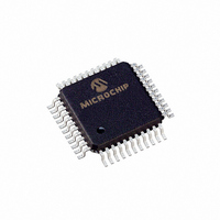
PIC16LC774-I/PQ Microchip Technology, PIC16LC774-I/PQ Datasheet - Page 121

PIC16LC774-I/PQ
Manufacturer Part Number
PIC16LC774-I/PQ
Description
44 PIN, 7KB OTP, 256 RAM, 33 I/O,
Manufacturer
Microchip Technology
Series
PIC® 16Cr
Specifications of PIC16LC774-I/PQ
Rohs Compliant
YES
Core Processor
PIC
Core Size
8-Bit
Speed
20MHz
Connectivity
I²C, SPI, UART/USART
Peripherals
Brown-out Detect/Reset, POR, PWM, WDT
Number Of I /o
33
Program Memory Size
7KB (4K x 14)
Program Memory Type
OTP
Ram Size
256 x 8
Voltage - Supply (vcc/vdd)
2.5 V ~ 5.5 V
Data Converters
A/D 10x12b
Oscillator Type
External
Operating Temperature
-40°C ~ 85°C
Package / Case
44-MQFP, 44-PQFP
Processor Series
PIC16LC
Core
PIC
Data Bus Width
8 bit
Data Ram Size
256 B
Interface Type
I2C, SPI, SSP, UART
Maximum Clock Frequency
20 MHz
Number Of Programmable I/os
33
Number Of Timers
3 bit
Operating Supply Voltage
2.5 V to 5.5 V
Maximum Operating Temperature
+ 85 C
Mounting Style
SMD/SMT
3rd Party Development Tools
52715-96, 52716-328, 52717-734
Development Tools By Supplier
ICE2000, DM163022
Minimum Operating Temperature
- 40 C
On-chip Adc
10 bit
Lead Free Status / RoHS Status
Lead free / RoHS Compliant
Eeprom Size
-
Lead Free Status / Rohs Status
Details
Available stocks
Company
Part Number
Manufacturer
Quantity
Price
Company:
Part Number:
PIC16LC774-I/PQ
Manufacturer:
Microchip Technology
Quantity:
10 000
11.4
The A/D conversion cycle requires 13T
tling time, and 12 T
A/D conversion clock is software selected. The four
possible options for T
TABLE 11-1
11.5
Figure 11-5
conversion. The port pins are configured as analog
inputs. The analog reference V
and the analog reference V
A/D interrupt is enabled, and the A/D conversion clock
is T
nel.
FIGURE 11-4: PERFORMING AN A/D CONVERSION
;
; Ensure that the required sampling time for the
; selected input channel has lapsed. Then the
; conversion may be started.
Operation
2 T
8 T
32 T
RC
Note 1: The RC source has a typical T
1999 Microchip Technology Inc.
RC
OSC
OSC
• 2 T
• 8 T
• 32 T
• Internal RC oscillator
BCF
BSF
CLRF
BSF
BCF
MOVLW
MOVWF
BSF
BSF
BSF
OSC
2: These values violate the minimum required T
3: For faster conversion times, the selection of another clock source is recommended.
4: When the device frequency is greater than 1 MHz, the RC A/D conversion clock source is only recommended if the conver-
. The conversion is performed on the AN0 chan-
AD Clock Source (T
sion will be performed during sleep.
Selecting the A/D Conversion Clock
A/D Conversions
OSC
OSC
OSC
shows an example that performs an A/D
PIR1, ADIF
STATUS, RP0
ADCON1
PIE1, ADIE
STATUS, RP0
0xC1
ADCON0
INTCON, PEIE
INTCON, GIE
ADCON0, GO
:
:
T
AD
AD
AD
ADCS<1:0>
for conversion. The source of the
vs. DEVICE OPERATING FREQUENCIES
are:
00
01
10
11
REF
AD
- is the device AV
)
REF
;Clear A/D Int Flag
;Select Page 1
;Configure A/D Inputs
;Enable A/D interrupt
;Select Page 0
;RC clock, A/D is on,
;Ch 0 is selected
;
;Enable Peripheral
;Enable All Interrupts
;Start A/D Conversion
;The ADIF bit will be
;set and the GO/DONE bit
;cleared upon completion-
;of the A/D conversion.
+ is the device AV
AD
time of 4 s for V
AD
: 1 T
2 - 6 s
100 ns
800 ns
Advance Information
20 MHz
AD
1.6 s
SS
for set-
AD
. The
(1,4)
(2)
(2)
time.
DD
DD
> 3.0V.
2 - 6 s
Note that these options are the same as those of the
8-bit A/D.
For correct A/D conversions, the A/D conversion clock
(T
of 1.6
derived from the device operating frequencies and the
A/D clock source selected.
The ADIF bit is set on the rising edge of the 14th T
The GO/DONE bit is cleared on the falling edge of the
14th T
400 ns
5 MHz
1.6 s
6.4 s
AD
) must be selected to ensure a minimum T
Device Frequency
AD
(1,4)
(2)
s.
.
Table 11-1
2 - 6 s
500 ns
8.0 s
4 MHz
2.0 s
shows the resultant T
PIC16C77X
(3)
(1,4)
(2)
DS30275A-page 121
2 - 6 s
1.25 MHz
24 s
1.6 s
6.4 s
AD
(3)
(1,4)
AD
times
time
AD
.


