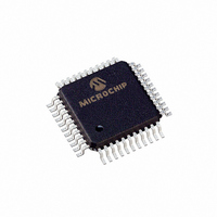
PIC16LC774-I/PQ Microchip Technology, PIC16LC774-I/PQ Datasheet - Page 41

PIC16LC774-I/PQ
Manufacturer Part Number
PIC16LC774-I/PQ
Description
44 PIN, 7KB OTP, 256 RAM, 33 I/O,
Manufacturer
Microchip Technology
Series
PIC® 16Cr
Specifications of PIC16LC774-I/PQ
Rohs Compliant
YES
Core Processor
PIC
Core Size
8-Bit
Speed
20MHz
Connectivity
I²C, SPI, UART/USART
Peripherals
Brown-out Detect/Reset, POR, PWM, WDT
Number Of I /o
33
Program Memory Size
7KB (4K x 14)
Program Memory Type
OTP
Ram Size
256 x 8
Voltage - Supply (vcc/vdd)
2.5 V ~ 5.5 V
Data Converters
A/D 10x12b
Oscillator Type
External
Operating Temperature
-40°C ~ 85°C
Package / Case
44-MQFP, 44-PQFP
Processor Series
PIC16LC
Core
PIC
Data Bus Width
8 bit
Data Ram Size
256 B
Interface Type
I2C, SPI, SSP, UART
Maximum Clock Frequency
20 MHz
Number Of Programmable I/os
33
Number Of Timers
3 bit
Operating Supply Voltage
2.5 V to 5.5 V
Maximum Operating Temperature
+ 85 C
Mounting Style
SMD/SMT
3rd Party Development Tools
52715-96, 52716-328, 52717-734
Development Tools By Supplier
ICE2000, DM163022
Minimum Operating Temperature
- 40 C
On-chip Adc
10 bit
Lead Free Status / RoHS Status
Lead free / RoHS Compliant
Eeprom Size
-
Lead Free Status / Rohs Status
Details
Available stocks
Company
Part Number
Manufacturer
Quantity
Price
Company:
Part Number:
PIC16LC774-I/PQ
Manufacturer:
Microchip Technology
Quantity:
10 000
5.0
The Timer1 module timer/counter has the following fea-
tures:
• 16-bit timer/counter
• Readable and writable (Both registers)
• Internal or external clock select
• Interrupt on overflow from FFFFh to 0000h
• Reset from CCP module trigger
Timer1 has a control register, shown in
Timer1 can be enabled/disabled by setting/clearing
control bit TMR1ON (T1CON<0>).
Figure 5-3
module.
Additional information on timer modules is available in
the
(DS33023).
FIGURE 5-1:
(Two 8-bit registers; TMR1H and TMR1L)
bit7
1999 Microchip Technology Inc.
bit 7-6: Unimplemented: Read as ’0’
bit 5-4: T1CKPS1:T1CKPS0: Timer1 Input Clock Prescale Select bits
bit 3:
bit 2:
bit 1:
bit 0:
U-0
PICmicro™
—
TIMER1 MODULE
is a simplified block diagram of the Timer1
11 = 1:8 Prescale value
10 = 1:4 Prescale value
01 = 1:2 Prescale value
00 = 1:1 Prescale value
T1OSCEN: Timer1 Oscillator Enable Control bit
1 = Oscillator is enabled
0 = Oscillator is shut off
Note: The oscillator inverter and feedback resistor are turned off to eliminate power drain
T1SYNC: Timer1 External Clock Input Synchronization Control bit
TMR1CS = 1
1 = Do not synchronize external clock input
0 = Synchronize external clock input
TMR1CS = 0
This bit is ignored. Timer1 uses the internal clock when TMR1CS = 0.
TMR1CS: Timer1 Clock Source Select bit
1 = External clock from pin RC0/T1OSO/T1CKI (on the rising edge)
0 = Internal clock (F
TMR1ON: Timer1 On bit
1 = Enables Timer1
0 = Stops Timer1
U-0
—
T1CON: TIMER1 CONTROL REGISTER (ADDRESS 10h)
Mid-Range
T1CKPS1 T1CKPS0 T1OSCEN T1SYNC
R/W-0
OSC
Reference
R/W-0
/4)
Figure
R/W-0
Advance Information
Manual,
5-1.
R/W-0
5.1
Timer1 can operate in one of these modes:
• As a timer
• As a synchronous counter
• As an asynchronous counter
The operating mode is determined by the clock select
bit, TMR1CS (T1CON<1>).
In timer mode, Timer1 increments every instruction
cycle. In counter mode, it increments on every rising
edge of the external clock input.
When the Timer1 oscillator is enabled (T1OSCEN is
set), the RC1/T1OSI and RC0/T1OSO/T1CKI pins
become inputs. That is, the TRISC<1:0> value is
ignored.
Timer1 also has an internal “reset input”. This reset can
be generated by the CCP module
TMR1CS TMR1ON
R/W-0
Timer1 Operation
R/W-0
bit0
R = Readable bit
W = Writable bit
U = Unimplemented bit,
- n = Value at POR reset
PIC16C77X
read as ‘0’
(Section
DS30275A-page 41
7.0).


