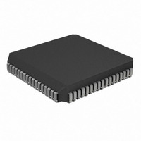
PIC16LC924-04/L Microchip Technology, PIC16LC924-04/L Datasheet - Page 41

PIC16LC924-04/L
Manufacturer Part Number
PIC16LC924-04/L
Description
IC,MICROCONTROLLER,8-BIT,PIC CPU,CMOS,LDCC,68PIN,PLASTIC
Manufacturer
Microchip Technology
Series
PIC® 16Cr
Specifications of PIC16LC924-04/L
Rohs Compliant
YES
Core Processor
PIC
Core Size
8-Bit
Speed
4MHz
Connectivity
I²C, SPI
Peripherals
LCD, POR, PWM, WDT
Number Of I /o
25
Program Memory Size
7KB (4K x 14)
Program Memory Type
OTP
Ram Size
176 x 8
Voltage - Supply (vcc/vdd)
2.5 V ~ 6 V
Data Converters
A/D 5x8b
Oscillator Type
External
Operating Temperature
0°C ~ 70°C
Package / Case
68-PLCC
Processor Series
PIC16LC
Core
PIC
Data Bus Width
8 bit
Data Ram Size
176 B
Interface Type
I2C, SPI
Maximum Clock Frequency
8 MHz
Number Of Programmable I/os
25
Number Of Timers
3
Operating Supply Voltage
2.5 V to 6 V
Maximum Operating Temperature
+ 70 C
Mounting Style
SMD/SMT
3rd Party Development Tools
52715-96, 52716-328, 52717-734
Development Tools By Supplier
ICE2000
Minimum Operating Temperature
0 C
On-chip Adc
8 bit, 5 Channel
Lead Free Status / RoHS Status
Lead free / RoHS Compliant
Eeprom Size
-
Lead Free Status / Rohs Status
Details
Other names
PIC16LC924-04/LR
PIC16LC924-04/LR
PIC16LC924-04/LR
Available stocks
Company
Part Number
Manufacturer
Quantity
Price
Company:
Part Number:
PIC16LC924-04/L
Manufacturer:
Microchip Technology
Quantity:
10 000
5.8
5.8.1
Any instruction which writes, operates internally as a
read followed by a write operation. The BCF and BSF
instructions, for example, read the register into the
CPU, execute the bit operation and write the result back
to the register. Caution must be used when these
instructions are applied to a port with both inputs and
outputs defined. For example, a BSF operation on bit5
of PORTB will cause all eight bits of PORTB to be read
into the CPU. Then the BSF operation takes place on
bit5 and PORTB is written to the output latches. If
another bit of PORTB is used as a bi-directional I/O pin
(e.g., bit0) and it is defined as an input at this time, the
input signal present on the pin itself would be read into
the CPU and rewritten to the data latch of this particular
pin, overwriting the previous content. As long as the pin
stays in the input mode, no problem occurs. However, if
bit0 is switched into output mode later on, the contents
of the data latch may now be unknown.
Reading the port register, reads the values of the port
pins. Writing to the port register writes the value to the
port latch. When using read-modify-write instructions
(ex. BCF, BSF) on a port, the value of the port pins is
read, the desired operation is done to this value, and
this value is then written to the port latch.
Example 5-8 shows the effect of two sequential
read-modify-write instructions on an I/O port.
FIGURE 5-11: SUCCESSIVE I/O OPERATION
1997 Microchip Technology Inc.
Instruction
Instruction
RB7:RB0
executed
fetched
I/O Programming Considerations
BI-DIRECTIONAL I/O PORTS
PC
Q1 Q2 Q3 Q4 Q1 Q2 Q3 Q4 Q1 Q2 Q3 Q4 Q1 Q2 Q3 Q4
MOVWF PORTB
write to
PORTB
PC
MOVF PORTB,W
MOVWF PORTB
write to
PORTB
PC + 1
T
MOVF PORTB,W
PD
Port pin
sampled here
NOP
PC + 2
EXAMPLE 5-8:
;Initial PORT settings: PORTB<7:4> Inputs
;
;PORTB<7:6> have external pull-ups and are
;not connected to other circuitry
;
;
;
;
;Note that the user may have expected the
;pin values to be 00pp ppp. The 2nd BCF
;caused RB7 to be latched as the pin value
;(high).
A pin actively outputting a Low or High should not be
driven from external devices at the same time in order
to change the level on this pin (“wired-or”, “wired-and”).
The resulting high output currents may damage the
chip.
5.8.2
The actual write to an I/O port happens at the end of an
instruction cycle, whereas for reading, the data must be
valid at the beginning of the instruction cycle
(Figure 5-11). Therefore, care must be exercised if a
write followed by a read operation is carried out on the
same I/O port. The sequence of instructions should be
such to allow the pin voltage to stabilize (load depen-
dent) before the next instruction which causes that file
to be read into the CPU is executed. Otherwise, the
previous state of that pin may be read into the CPU
rather than the new state. When in doubt, it is better to
separate these instructions with a NOP or another
instruction not accessing this I/O port.
BCF PORTB, 7
BCF PORTB, 6
BCF STATUS, RP1 ;
BSF STATUS, RP0 ;
BCF TRISB, 7
BCF TRISB, 6
PC + 3
NOP
NOP
SUCCESSIVE OPERATIONS ON I/O PORTS
Note:
This example shows a write to PORTB
followed by a read from PORTB.
Note that:
data setup time = (0.25T
where T
Therefore, at higher clock frequencies,
a write followed by a read may be prob-
lematic.
READ-MODIFY-WRITE
INSTRUCTIONS ON AN I/O
PORT
; 01pp pppp
; 10pp pppp
; 10pp pppp
; 10pp pppp
PIC16C9XX
T
PORT latch
----------
CY
PD
= instruction cycle
= propagation delay
PORTB<3:0> Outputs
DS30444E - page 41
PORT pins
---------
11pp pppp
11pp pppp
11pp pppp
10pp pppp
CY
- T
PD
)


