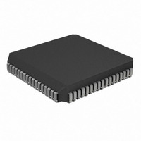
PIC18C601-I/L Microchip Technology, PIC18C601-I/L Datasheet - Page 82

PIC18C601-I/L
Manufacturer Part Number
PIC18C601-I/L
Description
IC,MICROCONTROLLER,8-BIT,PIC CPU,CMOS,LDCC,68PIN,PLASTIC
Manufacturer
Microchip Technology
Series
PIC® 18Cr
Datasheets
1.PIC16F616T-ISL.pdf
(8 pages)
2.PIC18C601-IL.pdf
(320 pages)
3.PIC18C601-IL.pdf
(10 pages)
4.PIC18C601-IL.pdf
(10 pages)
Specifications of PIC18C601-I/L
Rohs Compliant
YES
Core Processor
PIC
Core Size
8-Bit
Speed
25MHz
Connectivity
EBI/EMI, I²C, SPI, UART/USART
Peripherals
Brown-out Detect/Reset, LVD, POR, PWM, WDT
Number Of I /o
26
Program Memory Type
ROMless
Ram Size
1.5K x 8
Voltage - Supply (vcc/vdd)
4.2 V ~ 5.5 V
Data Converters
A/D 8x10b
Oscillator Type
External
Operating Temperature
-40°C ~ 85°C
Package / Case
68-PLCC
Processor Series
PIC18C
Core
PIC
Data Bus Width
8 bit
Data Ram Size
1.5 KB
Interface Type
3-Wire, I2C, SPI, USART
Maximum Clock Frequency
25 MHz
Number Of Programmable I/os
47
Number Of Timers
1 x 16 bit
Operating Supply Voltage
2 V to 5.5 V
Maximum Operating Temperature
+ 85 C
Mounting Style
SMD/SMT
3rd Party Development Tools
52715-96, 52716-328, 52717-734, 52712-325, EWPIC18
Development Tools By Supplier
DV164005, ICE4000, DV164136
Minimum Operating Temperature
- 40 C
On-chip Adc
10 bit
Lead Free Status / RoHS Status
Lead free / RoHS Compliant
For Use With
AC164309 - MODULE SKT FOR PM3 44PLCCXLT68L1 - SOCKET TRANSITION ICE 68PLCCAC174007 - MODULE SKT PROMATEII 68PLCC
Eeprom Size
-
Program Memory Size
-
Lead Free Status / Rohs Status
Details
Other names
PIC18C601I/L
Available stocks
Company
Part Number
Manufacturer
Quantity
Price
Company:
Part Number:
PIC18C601-I/L
Manufacturer:
Microchip
Quantity:
229
Company:
Part Number:
PIC18C601-I/L
Manufacturer:
Microchip Technology
Quantity:
10 000
- PIC16F616T-ISL PDF datasheet
- PIC18C601-IL PDF datasheet #2
- PIC18C601-IL PDF datasheet #3
- PIC18C601-IL PDF datasheet #4
- Current page: 82 of 320
- Download datasheet (6Mb)
PIC18C601/801
6.3.4
This mode allows Table Writes to word-wide external
memories that have byte selection capabilities. This
generally includes word-wide FLASH devices and
word-wide static RAM devices.
During a TBLWT cycle, the TABLAT data is presented
on the upper and lower byte of the AD<15:0> bus.
The WRH line is strobed for each write cycle and the
FIGURE 6-10:
DS39541A-page 82
AD<15:0>
A<19:16>
Instruction
Execution
Memory
WRH
WRL
Cycle
ALE
BA0
OE
UB
LB
’1’
16-BIT EXTERNAL TABLE WRITE
(BYTE SELECT MODE)
Q1
Opcode Fetch
3AAAh
from 007554h
INST(PC-2)
TBLWT*+
Q2
0h
Q3 Q4
TBLWT EXTERNAL INTERFACE TIMING (16-BIT BYTE SELECT MODE)
000Dh
MOVWF TABLAT
TBLWT*+ Cycle1 TBLWT*+ Cycle2
Q1
Opcode Fetch
from 007556h
3AABh
Q2
0h
Q3 Q4
6FF4h
Advance Information
Q1
CF33h
TBLWT 56h
to 199E66h
Q2
Ch
Q3 Q4
5656h
WRL line is unused. The BA0 or UB or UL lines are
used to select the byte to be written, based on the LSb
of the TBLPTR.
JEDEC standard flash memories will require a I/O port
line to become a BYTE/WORD input signal and will
use the BA0 signal as a byte address. JEDEC stan-
dard static RAM memories will use the UB or UL sig-
nals to select the byte.
Figure 6-10 shows the timing associated with this mode.
Q1
Opcode Fetch
3AACh
from 007558h
MOVWF
TBLWT*
Q2
0h
Q3 Q4
000Ch
Q1
TBLWT* Cycle1
Opcode Fetch
from 00755Ah
MOVLW 55h
3AADh
Q2
0h
Q3 Q4
2001 Microchip Technology Inc.
0E55h
Q1
TBLWT* Cycle2
CF33h
TBLWT 92h
to 199E67h
Q2
Ch
Q3 Q4
9292h
Related parts for PIC18C601-I/L
Image
Part Number
Description
Manufacturer
Datasheet
Request
R

Part Number:
Description:
IC, 8BIT MCU, PIC18F, 40MHZ, LCC-44
Manufacturer:
Microchip Technology
Datasheet:

Part Number:
Description:
IC, 8BIT MCU, PIC18LF, 40MHZ, PLCC-64
Manufacturer:
Microchip Technology
Datasheet:

Part Number:
Description:
IC, 8BIT MCU, PIC18F, 64MHZ, TQFP-80
Manufacturer:
Microchip Technology
Datasheet:

Part Number:
Description:
MCU, MPU & DSP Development Tools CAN/LIN PICtail Plus Daughter Board
Manufacturer:
Microchip Technology
Datasheet:

Part Number:
Description:
IC, 8BIT MCU, PIC18F, 64MHZ, DIP-40
Manufacturer:
Microchip Technology
Datasheet:

Part Number:
Description:
IC, 8BIT MCU, PIC18LF, 40MHZ, PLCC-64
Manufacturer:
Microchip Technology
Datasheet:

Part Number:
Description:
IC, 8BIT MCU, PIC18F, 64MHZ, TQFP-64
Manufacturer:
Microchip Technology

Part Number:
Description:
IC, 8BIT MCU, PIC18F, 64MHZ, TQFP-80
Manufacturer:
Microchip Technology

Part Number:
Description:
8KB, Flash, 768bytes-RAM, 36I/O, 8-bit Family,nanowatt XLP 40 UQFN 5x5x0.5mm TUB
Manufacturer:
Microchip Technology
Datasheet:

Part Number:
Description:
8KB, Flash, 768bytes-RAM, 36I/O, 8-bit Family,nanowatt XLP 40 UQFN 5x5x0.5mm TUB
Manufacturer:
Microchip Technology

Part Number:
Description:
16KB, Flash, 768bytes-RAM, 36I/O, 8-bit Family,nanowatt XLP 40 UQFN 5x5x0.5mm TU
Manufacturer:
Microchip Technology
Datasheet:

Part Number:
Description:
16KB, Flash, 768bytes-RAM, 36I/O, 8-bit Family,nanowatt XLP 40 UQFN 5x5x0.5mm TU
Manufacturer:
Microchip Technology

Part Number:
Description:
32KB, Flash, 1536bytes-RAM, 36I/O, 8-bit Family,nanowatt XLP 40 UQFN 5x5x0.5mm T
Manufacturer:
Microchip Technology
Datasheet:

Part Number:
Description:
32KB, Flash, 1536bytes-RAM, 36I/O, 8-bit Family,nanowatt XLP 40 UQFN 5x5x0.5mm T
Manufacturer:
Microchip Technology

Part Number:
Description:
64KB, Flash, 3968bytes-RAM, 36I/O, 8-bit Family,nanowatt XLP 40 UQFN 5x5x0.5mm T
Manufacturer:
Microchip Technology
Datasheet:


