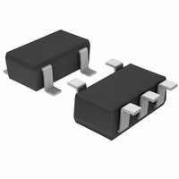
BD7411G-TR Rohm Semiconductor, BD7411G-TR Datasheet

BD7411G-TR
Specifications of BD7411G-TR
Available stocks
Related parts for BD7411G-TR
BD7411G-TR Summary of contents
Page 1
... In addition to regular single-output Hall ICs, We offers a line up of dual-output units with a reverse output terminal (active High). Features 1) Bipolar detection 2) Micropower operation (small current using intermittent operation method)(BD7411G is excluded.) 3) Ultra-compact CSP4 package (BU52001GUL,BU52015GUL) 4) Ultra-Small outline package HVSOF5 (BU52011HFV,BU52021HFV) 5) Ultra-Small outline package SSON004X1216 (BU52051NVXV) ...
Page 2
... OUT Power Dissipation Pd Operating Temperature Range T opr Storage Temperature Range T stg 9. Not to exceed Pd 10. Reduced by5.36mW for each increase mounted on 70mm 70 mm 1.6mm Glass-epoxy PCB BD7411G (Ta=25 ) PARAMETERS SYMBOL V Power Supply Voltage DD I Output Current OUT Power Dissipation Pd Operating Temperature Range ...
Page 3
Magnetic, Electrical Characteristics BU52001GUL (Unless otherwise specified, V PARAMETERS SYMBOL Power Supply Voltage opS Operate Point B opN B rpS Release Point B rpN B hysS Hysteresis B hysN Period T Output High Vol age V OH ...
Page 4
BU52015GUL (Unless otherwise specified, PARAMETERS SYMBOL Power Supply Voltage V B Operate Point B opN B Release Point B B hysS Hysteresis B hysN Period T Output High Vol age V Output Low Voltage V Supply Current 1 I DD1(AVG) ...
Page 5
BU52051NVX , BU52011HFV (Unless otherwise specified, V PARAMETERS SYMBOL Power Supply Voltage V B Operate Point B B Release Point B B Hysteresis B Period Output High Vol age V Output Low Voltage V Supply Current 1 I DD1(AVG) Supply ...
Page 6
... BD7411G (Unless otherwise specified, V PARAMETERS SYMBOL Power Supply Voltage opS Operate Point B opN B rpS Release Point B rpN B hysS Hysteresis B hysN Output High Vol age V OH Output Low Voltage V OL Supply Current Magnetic flux density 1mT=10Gauss Positive (“+”) polarity flux is defined as the magnetic flux from south pole which is direct toward to the branded face of the sensor ...
Page 7
... GND Fig.4 V measurement circuit VDD C GND Fig.5 I measurement circuit VDD OUT V BU52001GUL, BU52021HFV, BU52025G, BD7411G VDD BU52015GUL, BU52051NVX, BU52011HFV OUT I V OUT BU52001GUL, BU52021HFV, BU52025G, BD7411G BU52015GUL, BU52051NVX, BU52011HFV OUT V I OUT BU52001GUL,BU52015GUL,BU52051NVX, VDD OUT BU52011HFV, BU52021HFV, BU52025G BD7411G 7/20 200 ...
Page 8
Technical (Reference) Data BU52001GUL (V =2.4V 3.3V type) DD 8.0 6.0 V =3.0V DD Bop S 4.0 2.0 Brp S 0.0 -2.0 Brp N -4.0 Bop N -6.0 -8.0 -60 -40 - 100 AMBIENT TEMPERATURE ...
Page 9
... Ambient temperature 100 25° 2.0 2.4 2.8 3.2 3.6 4.0 SUPPLY VOLTAGE [V] Fig.21 T – Supply voltage P BD7411G (V =4.5V 5.5V type) DD 8.0 6.0 Bop S V =5.0V DD 4.0 2.0 Brp S 0.0 Brp N -2.0 -4.0 Bop N -6.0 -8.0 -60 -40 - 100 AMBIENT TEMPERATURE [ ] Fig.24 Bop,Brp– ...
Page 10
Block Diagram BU52001GUL TIMING LOGIC HALL ELEMENT ˜ PIN No. PIN NAME FUNCTION A1 POWER SUPPLY VDD A2 GROUND GND B1 OUTPUT OUT B2 N.C. BU52015GUL VDD TIMING LOGIC HALL ELEMENT ˜ PIN No. PIN NAME FUNCTION A1 OUT1 Output ...
Page 11
BU52051NVX TIMING LOGIC HALL ELEMENT ˜ PIN No. PIN NAME FUNCTION 1 OUT OUTPUT 2 GND GROUND 3 N.C. 4 VDD POWER SUPPLY BU52011HFV,BU52021HFV TIMING LOGIC HALL ELEMENT ˜ PIN No. PIN NAME FUNCTION 1 N.C. 2 GND GROUND 3 ...
Page 12
... BU52025G TIMING LOGIC HALL ELEMENT ˜ PIN No. PIN NAME FUNCTION 1 N.C. 2 GND GROUND 3 N.C. 4 VDD POWER SUPPLY 5 OUT OUTPUT BD7411G TIMING LOGIC REG HALL ELEMENT ˜ PIN No. PIN NAME FUNCTION 1 N.C. 2 GND GROUND 3 N.C. 4 OUT OUTPUT 5 VDD POWER SUPPLY DD 4 Fig.32 COMMENT OPEN or Short to GND ...
Page 13
... Reference period: 50ms (MAX100ms) t Reference startup time BD7411G don’t adopts an intermittent operation method. The Hall elements form an equivalent Wheatstone (resistor) bridge circuit. Offset voltage may be generated by a differential in this bridge resistance, or can arise from changes in resistance due to package or bonding stress. A dynamic offset cancellation circuit is employed to cancel this offset voltage ...
Page 14
Field Detection Mechanism Flux The Hall IC cannot detect magnetic fields that run horizontal to the package top layer. Be certain to configure the Hall IC so that the magnetic field is perpendicular to the top ...
Page 15
... To accommodate the system design, the Hall IC output read should be programmed within 100ms of power ON, but after the time allowed for the period ambient temperature and supply voltage. BD7411G don’t adopts an intermittent operation method. Magnet Selection ...
Page 16
Position of the Hall Effect IC(Reference) VCSP50L1 0.55 0.55 0.8 0.35 0.2 Footprint dimensions (Optimize footprint dimensions to the board design and soldering condition) VCSP50L1 Terminal Equivalent Circuit Diagram OUT , OUT1, OUT2 Fig.41 HVSOF5 SSON004X1216 0.6 0.6 0.8 0.2 ...
Page 17
Operation Notes 1 Absolute maximum ratings Exceeding the absolute maximum ratings for supply voltage, operating conditions, etc. may result in damage to or destruction of the IC. Because the source (short mode or open mode) cannot be identified if the ...
Page 18
Exposure to strong light Exposure to halogen lamps, UV and other strong light sources may cause the IC to malfunction. If the IC is subject to such exposure, provide a shield or take other measures to protect it from ...
Page 19
SSOP5 <Dimensions> + ° 6 2.9±0.2 ° 4 ° − +0.05 0.13 −0.03 +0.05 0.42 −0.04 0.95 0.1 (Unit:mm) HVSOF5 <Dimensions> 1.6±0.05 0.8 0.3 1.0±0. 0.13±0. ...
Page 20
Catalog No.08T155A '08.7 ROHM © ...


