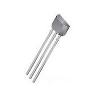
A1201EUA-T Allegro Microsystems Inc, A1201EUA-T Datasheet - Page 9

A1201EUA-T
Manufacturer Part Number
A1201EUA-T
Description
IC SW CONTINUE TIME BIPO 3-SIP
Manufacturer
Allegro Microsystems Inc
Type
Bipolar Latchr
Datasheet
1.A1203EUA-T.pdf
(13 pages)
Specifications of A1201EUA-T
Sensing Range
50G Trip, -50G Release
Voltage - Supply
3.8 V ~ 24 V
Current - Supply
7.5mA
Current - Output (max)
25mA
Output Type
Digital, Open Drain
Features
Regulated Voltage
Operating Temperature
-40°C ~ 85°C
Package / Case
3-SIP
Magnetic Type
Bipolar
Operating Supply Voltage (min)
3.8V
Operating Supply Voltage (typ)
5/9/12/15/18V
Operating Supply Voltage (max)
24V
Output Current
25mA
Mag Sensor Operate Point (g)
50Gs
Mag Sensor Release Point (g)
-50Gs
Mag Sensor Hysteresis(g)
30Gs
Package Type
Ultra Mini SIP
Pin Count
3
Mounting
Through Hole
Operating Temp Range
-40C to 85C
Operating Temperature Classification
Industrial
Lead Free Status / RoHS Status
Lead free / RoHS Compliant
A1201
the field is reduced beyond the B
back to the low state.
The typical output behavior of the A1201 device is latching.
That is, switching to the low state when the magnetic field at the
Hall element exceeds the operate point threshold, B
point, the output voltage is V
is reduced to below the release point threshold, B
output, V
are specified in the Magnetic Characteristics table, on page 3.
Note that, as shown in figure 1, these switchpoints can lie in
either north or south polarity ranges.
The A1201 is designed to attain a small hysteresis, and thereby
provide more sensitive switching. Although this means that
true latching behavior cannot be guaranteed in all cases, proper
switching can be ensured by use of both south and north mag-
netic fields, as in a ring magnet. The hysteresis of the A1201
allows clean switching of the output, even in the presence of
external mechanical vibration and electrical noise.
Figure 2. Continuous-Time Application, B < B
Position 1, power is applied to the device. Position 2, the output assumes the correct state at a time prior to the maximum Power-On Time, t
The case shown is where the correct output state is HIGH . Position 3, t
valid, a control unit reads the output. Position 5, power is removed from the device.
OUT
, goes high. The values of the magnetic parameters
OUT(SAT)
V
V
OUT
CC
OP
level, the device switches
. When the magnetic field
1
RP
.. This figure illustrates the use of a quick cycle for chopping V
RP
OP
, the device
. At this
2
t
PO(max)
PO(max)
3
Continuous-Time Bipolar Switch
Bipolar devices adopt an indeterminate output state when pow-
ered-on in the absence of a magnetic field or in a field that lies
within the hysteresis band of the device.
For more information on Bipolar switches, refer to Application
Note 27705, Understanding Bipolar Hall Effect Sensor ICs.
CONTINUOUS-TIME BENEFITS
Continuous-time devices, such as the A1201, offer the fastest
available power-on settling time and frequency response. Due to
offsets generated during the IC packaging process, continuous-
time devices typically require programming after packaging to
tighten magnetic parameter distributions. In contrast, chopper-
stabilized switches employ an offset cancellation technique
on the chip that eliminates these offsets without the need for
after-packaging programming. The tradeoff is a longer settling
time and reduced frequency response as a result of the chopper-
stabilization offset cancellation algorithm.
has elapsed. The device output is valid. Position 4, after the output is
Output Sampled
4
5
115 Northeast Cutoff, Box 15036
Allegro MicroSystems, Inc.
Worcester, Massachusetts 01615-0036 (508) 853-5000
www.allegromicro.com
CC
in order to conserve battery power.
t
t
PO(max)
.
9


