SI8800EDB-T2-E1 Vishay, SI8800EDB-T2-E1 Datasheet

N-CHANNEL 20-V (D-S) MOSFET

SI8800EDB-T2-E1

Manufacturer Part Number
SI8800EDB-T2-E1
Description
N-CHANNEL 20-V (D-S) MOSFET
Manufacturer
Vishay
Series
TrenchFET®r
Datasheet

Specifications of SI8800EDB-T2-E1

Fet Type
MOSFET N-Channel, Metal Oxide
Fet Feature
Logic Level Gate
Rds On (max) @ Id, Vgs
80 mOhm @ 1A, 4.5V
Drain To Source Voltage (vdss)
20V
Vgs(th) (max) @ Id
1V @ 250µA
Gate Charge (qg) @ Vgs
8.3nC @ 8V
Power - Max
500mW
Mounting Type
Surface Mount
Package / Case
4-MICRO FOOT®CSP
Gate Charge Qg
5.5 nC
Minimum Operating Temperature
- 55 C
Transistor Polarity
N-Channel
Resistance Drain-source Rds (on)
0.095 Ohms
Forward Transconductance Gfs (max / Min)
10 S
Drain-source Breakdown Voltage
20 V
Gate-source Breakdown Voltage
8 V
Continuous Drain Current
2.8 A
Power Dissipation
900 mW
Maximum Operating Temperature
+ 125 C
Mounting Style
SMD/SMT
Lead Free Status / RoHS Status
Lead free / RoHS Compliant
Current - Continuous Drain (id) @ 25° C
-
Lead Free Status / Rohs Status
Lead free / RoHS Compliant
Other names
SI8800EDB-T2-E1TR

Available stocks

Company
Part Number
Manufacturer
Quantity
Price
Part Number:
SI8800EDB-T2-E1
Manufacturer:
VISHAY
Quantity:
300
Part Number:
SI8800EDB-T2-E1
Manufacturer:
VISHAY/威世
Quantity:
20 000
Company:
Part Number:
SI8800EDB-T2-E1
Quantity:
70 000
Notes:
a. Surface mounted on 1" x 1" FR4 board with full copper, t = 5 s.
b. Surface mounted on 1" x 1" FR4 board with minimum copper, t = 5 s.
c. Refer to IPC/JEDEC (J-STD-020C), no manual or hand soldering.
d. Maximum under steady state conditions is 185 °C/W.
e. Maximum under steady state conditions is 330 °C/W.
Document Number: 66700
S10-1046-Rev. A, 03-May-10
Ordering Information: Si8800EDB-T2-E1 (Lead (Pb)-free and Halogen-free)
ABSOLUTE MAXIMUM RATINGS T
Parameter
Drain-Source Voltage
Gate-Source Voltage
Continuous Drain Current (T
Pulsed Drain Current
Continuous Source-Drain Diode Current
Maximum Power Dissipation
Operating Junction and Storage Temperature Range
Soldering Recommendations (Peak Temperature)
THERMAL RESISTANCE RATINGS
Parameter
Maximum Junction-to-Ambient
PRODUCT SUMMARY
V
DS
20
(V)
Device Marking: 800
Bump Side View
S
S
2
3
0.080 at V
0.090 at V
0.105 at V
0.150 at V
R
G
D
MICRO FOOT
DS(on)
xxx = Date/Lot Traceability Code
1
4
GS
GS
GS
GS
J
(Ω)
= 4.5 V
= 2.5 V
= 1.8 V
= 1.5 V
= 150 °C)
a, d
b, e
Backside View
N-Channel 20 V (D-S) MOSFET
I
D
2.8
2.6
2.4
2.0
(A)
a
c
T
T
T
T
T
T
T
T
T
T
t ≤ 5 s
A
A
A
A
A
A
A
A
A
A
A
= 25 °C
= 70 °C
= 25 °C
= 70 °C
= 25 °C
= 25 °C
= 25 °C
= 70 °C
= 25 °C
= 70 °C
= 25 °C, unless otherwise noted
Q
3.2 nC
g
(Typ.)
Symbol
R
thJA
Symbol
T
J
V
V
I
P
, T
DM
I
I
DS
GS
D
S
D
FEATURES
APPLICATIONS
stg
• Halogen-free According to IEC 61249-2-21
• TrenchFET
• Ultra Small 0.8 mm x 0.8 mm Outline
• Ultra Thin 0.357 mm Height
• Typical ESD Protection 1500 V
• Portable Devices such as Cell Phones,
Definition
Compliant to RoHS Directive 2002/95/EC
Smart Phones and MP3 Players
- Load Switch
- Small Signal Switch
Typical
105
200
®
Power MOSFET
- 55 to 150
Limit
2.8
2.2
2.0
1.6
0.7
0.4
0.9
0.6
0.5
0.3
260
± 8
20
15
a
a
b
b
a
b
a
a
b
b
Maximum
G
135
260
Vishay Siliconix
Si8800EDB
R
www.vishay.com
°C/W
Unit
Unit
°C
W
V
A
D
S
1

Related parts for SI8800EDB-T2-E1

SI8800EDB-T2-E1 Summary of contents

Page 1

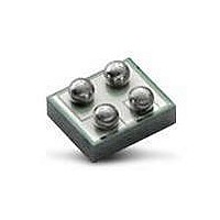
... Backside View Device Marking: 800 xxx = Date/Lot Traceability Code Ordering Information: Si8800EDB-T2-E1 (Lead (Pb)-free and Halogen-free) ABSOLUTE MAXIMUM RATINGS T Parameter Drain-Source Voltage Gate-Source Voltage Continuous Drain Current (T = 150 °C) J Pulsed Drain Current Continuous Source-Drain Diode Current Maximum Power Dissipation Operating Junction and Storage Temperature Range ...

Page 2

... Si8800EDB Vishay Siliconix SPECIFICATIONS °C, unless otherwise noted J Parameter Static Drain-Source Breakdown Voltage V Temperature Coefficient DS V Temperature Coefficient GS(th) Gate-Source Threshold Voltage Gate-Source Leakage Zero Gate Voltage Drain Current a On-State Drain Current a Drain-Source On-State Resistance a Forward Transconductance b Dynamic Total Gate Charge ...

Page 3

... On-Resistance vs. Drain Current Document Number: 66700 S10-1046-Rev. A, 03-May- ° - 1 2.0 2.5 3 Si8800EDB Vishay Siliconix T = 150 ° ° Gate-to-Source Voltage (V) GS Gate Current vs. Gate-Source Voltage ° 125 ° °C C 0.3 0.6 0.9 1 Gate-to-Source Voltage (V) GS Transfer Characteristics Total Gate Charge (nC) ...

Page 4

... Si8800EDB Vishay Siliconix TYPICAL CHARACTERISTICS 25 °C, unless otherwise noted 1.4 1.3 1.2 1 1.0 0.9 0.8 0 Junction Temperature (°C) J On-Resistance vs. Junction Temperature 0. 0. ° 0. 0 ° 0. Gate-to-Source Voltage (V) GS On-Resistance vs. Gate-to-Source Voltage www.vishay.com 0.1 75 100 125 150 ...

Page 5

... V at which DS(on) Safe Operating Area, Junction-to-Ambient 0.8 0.6 0.4 0.2 0.0 100 125 150 25 = 150 °C, using junction-to-ambient thermal resistance, and is more useful in settling the upper Si8800EDB Vishay Siliconix 100 μ 100 ms 100 is specified 50 75 100 125 T - Ambient Temperature (°C) A Power Derating www ...

Page 6

... Si8800EDB Vishay Siliconix TYPICAL CHARACTERISTICS 25 °C, unless otherwise noted 1 Duty Cycle = 0.5 0.2 0.1 0.1 0.05 0.02 Single Pulse 0. Normalized Thermal Transient Impedance, Junction-to-Ambient (On 1" x 1" FR4 board with maximum copper) 1 Duty Cycle = 0.5 0.2 0.1 0.1 0.05 0.02 Single Pulse ...

Page 7

... Note 4 Solder Mask ~ Ø 0.215 Millimeters Nom. Max. 0.357 0.400 0.157 0.187 0.200 0.213 0.175 0.185 0.400 0.200 0.220 0.800 0.840 Si8800EDB Vishay Siliconix Inches Min. Nom. Max. 0.0124 0.0141 0.0157 0.0050 0.0062 0.0074 0.0074 0.0079 0.0084 ...

Page 8

... Vishay product could result in personal injury or death. Customers using or selling Vishay products not expressly indicated for use in such applications their own risk and agree to fully indemnify and hold Vishay and its distributors harmless from and against any and all claims, liabilities, expenses and damages arising or resulting in connection with such use or sale, including attorneys fees, even if such claim alleges that Vishay or its distributor was negligent regarding the design or manufacture of the part ...

Related keywords