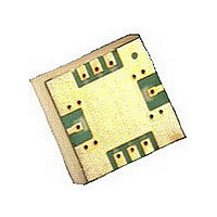
AMMP-5620-TR2G Avago Technologies US Inc., AMMP-5620-TR2G Datasheet - Page 2

AMMP-5620-TR2G
Manufacturer Part Number
AMMP-5620-TR2G
Description
6-20 GHz High Gain Amp In SMT Pkg
Manufacturer
Avago Technologies US Inc.
Datasheet
1.AMMP-5620-TR2G.pdf
(12 pages)
Specifications of AMMP-5620-TR2G
Current - Supply
95mA
Frequency
6GHz ~ 20GHz
Gain
17.5dB
Noise Figure
5.1dB
P1db
14.8dBm
Package / Case
8-SMD
Rf Type
General Purpose
Test Frequency
18GHz
Voltage - Supply
5V
Number Of Channels
1
Frequency (max)
20GHz
Power Supply Requirement
Single
Single Supply Voltage (typ)
5V
Package Type
SMT
Dual Supply Voltage (min)
Not RequiredV
Dual Supply Voltage (typ)
Not RequiredV
Dual Supply Voltage (max)
Not RequiredV
Supply Current
130mA
Pin Count
8
Mounting
Surface Mount
Lead Free Status / RoHS Status
Lead free / RoHS Compliant
Lead Free Status / RoHS Status
Lead free / RoHS Compliant
Available stocks
Company
Part Number
Manufacturer
Quantity
Price
Part Number:
AMMP-5620-TR2G
Manufacturer:
AVAGO/安华高
Quantity:
20 000
Table 1. Absolute Maximum Ratings
Notes:
1. Operation in excess of any one of these conditions may result in permanent damage to this device.
Table 2. DC Specifications
Notes:
1. Ambient operation temperature T
2. Channel-to-board Thermal Resistance is measured using Infrared Microscopy method.
Table 3. RF Specifications
Notes:
1. Typical value determined from a sample size of 500 parts from 2 wafers.
2. Small/large signal data measured in a fully de-embedded test fixture at T
3. Specifications are derived from measurements in a 50 Ohm test environment. Aspects of the amplifier performance may be improved over a
4. All tested parameters guaranteed with measurement accuracy ± 0.5 dB for NF and ± 1.0 dB for gain.
2
Symbol
V
I
P
P
T
T
T
Symbol
V
I
q
Symbol
|S2|
RLin
RLout
|S2|
PdB
OIP3
NF
dd
dd
ch
stg
max
dd
dc
in
dd
ch-b
The absolute maximum ratings for Vdd, Idd, Pdc and Pin were determined at an ambient temperature of 25°C unless noted otherwise.
narrower bandwidth by application of additional conjugate, linearity, or low noise matching.
2
2
Parameters and Test Conditions
Positive Drain Voltage
Total Drain Current
DC Power Dissipation
RF CW Input Power
Operating Channel Temperature
Storage Case Temperature
Maximum Assembly Temperature (20 sec max)
Parameters and Test Conditions
Recommended Drain Supply Voltage
Total Drain Supply Current
Thermal Resistance
Parameters and Test Conditions
Small signal Gain
Input Return Loss
Output Return Loss
Reverse Isolation
Output Power at dB Gain Compression
Output 3rd Order Intercept Point
Noise Figure
[,4]
[2,3]
[,4]
[1]
[2]
(T
A
A
= 25°C unless otherwise noted.
= 25
[1]
°
C, Freq = 18GHz, Vdd = 5V, Idd = 95mA)
Unit
V
mA
°C/W
Unit
dB
dB
dB
dB
dBm
dBm
dB
Minimum
-
70
-
Minimum
5.5
-
-
-
-
-
-
Unit
V
mA
W
dBm
°C
°C
°C
A
= 25 degree Celsius.
Minimum
-
-
-
-
-
-65
-
Typical
5
95
28
Typical
7.5
.5
.6
-43.0
4.8
22.5
5.
Maximum
7.5
35
.0
20
+50
+50
+260
Maximum
-
30
-
Maximum
9.5
-
-
-
-
-
7.0


