IPR-PCIE/1 Altera, IPR-PCIE/1 Datasheet
IPR-PCIE/1
Specifications of IPR-PCIE/1


Related parts for IPR-PCIE/1


IPR-PCIE/1 Summary of contents
Page 1
... Innovation Drive San Jose, CA 95134 (408) 544-7000 www.altera.com PCI Express Compiler User Guide MegaCore Version: Document Version: Document Date: 6.1 6.1 rev. 2 December 2006 ...
Page 2
... Altera Corporation in the U.S. and other countries. All other product or service names are the property of their respective holders. Al- tera products are protected under numerous U ...
Page 3
... About This User Guide Revision History ....................................................................................................................................... ix How to Contact Altera ............................................................................................................................. xi Typographic Conventions ..................................................................................................................... xii Chapter 1. About This Compiler Release Information ............................................................................................................................... 1–1 Device Family Support ......................................................................................................................... 1–1 New in PCI Express Compiler Version 6.1 ........................................................................................ 1–2 Features ................................................................................................................................................... 1–2 General Description ............................................................................................................................... 1–3 Testbench & Example Designs: Simple DMA and Chaining DMA .......................................... 1–5 OpenCore Plus Evaluation .............................................................................................................. 1– ...
Page 4
... PHY Interface Signals ......................................................................................................... 4–11 8-bit PHY Interface Signals ........................................................................................................... 4–13 Selecting an External PHY .................................................................................................................. 4–15 External PHY Constraint Support ..................................................................................................... 4–16 Using External PHYs With the Stratix GX Device Family ....................................................... 4–17 iv PCI Express Compiler User Guide PCI Express Compiler Version 6.1 Altera Corporation December 2006 ...
Page 5
... Content with Data Payload ................................................................................................................. B–2 Appendix C. Test Port Interface Signals Test-Out Interface Signals for x1 and x4 MegaCore Functions .......................................................................................................... C–2 Test-Out Interface Signals for x8 MegaCore Functions ................................................................ C–19 Test-In Interface .................................................................................................................................. C–22 Altera Corporation December 2006 PCI Express Compiler Version 6.1 PCI Express Compiler User Guide v ...
Page 6
... Contents vi PCI Express Compiler User Guide PCI Express Compiler Version 6.1 Altera Corporation December 2006 ...
Page 7
... June 2005 2 December April 2006 October 2005 June 2005 3 December 2006 April 2006 October 2005 June 2005 Altera Corporation December 2006 About This User Guide 6.1 ● Added support for the Stratix ● Updated version and performance information 2.1.0 ● Rearranged content ● ...
Page 8
... Updated ECRC to include ECRC support for x8 1.0.0 Updated ECRC noting no support for x8 ● ● First release 2.1.0 ● Minor format changes throughout user guide rev 2 PCI Express Compiler Version 6.1 Changes Made PHYs”, added for external PHY support Procedure Procedure Altera Corporation December 2006 ...
Page 9
... How to Contact For the most up-to-date information about Altera Altera website at www.altera.com. For technical support on this product, Altera go to www.altera.com/mysupport. For additional information about Altera products, consult the sources shown below. Information Type Technical support www.altera.com/mysupport/ (800) 800-EPLD (3753) (7:00 a.m. to 5:00 p.m. Pacific Time) Product literature www ...
Page 10
... PCI Express Compiler User Guide Meaning , \qdesigns directory, d: drive, chiptrip.gdf file. MAX , PIA , input. Active-low signals are denoted by suffix c:\qdesigns\tutorial\chiptrip.gdf ), as well as logic function names (for example, BEGIN PCI Express Compiler Version 6.1 , data1 n , e.g., resetn . . Also, sections are TRI Altera Corporation December 2006 ...
Page 11
... Altera Corporation December 2006 1. About This Compiler provides information about this release of the Altera Item ® functions provide either full or preliminary support for target Full support means the MegaCore function meets all functional and timing requirements for the device family and may be used in ...
Page 12
... Extensive external PHY support for the x1 and x4 MegaCore ● functions Compliance for PCI Express Base Specification 1.1 Easy integration into customer design Functional simulation models for use in Altera-supported ● VHDL and Verilog HDL simulators Simple DMA example design ● High performance chaining DMA example design ● ...
Page 13
... PCI Express endpoints, including non- Description transparent bridges, or truly unique designs combining multiple PCI Express components in a single Altera device. The PCI Express MegaCore functions are PCI Express Base Specification Revision 1.1 or PCI Express™ Base Specification Revision 1.0a compliant, and implement all required and most optional features of the specification for the transaction, data link, and physical layers ...
Page 14
... General Description Figure 1–1. Example PCI Express System Optimized for Altera devices, the PCI Express Compiler supports all memory, I/O, configuration, and message transactions. The MegaCore functions have a highly optimized application interface to achieve maximum effective throughput. Because the Compiler is parameterizable, you can customize them to meet design requirements ...
Page 15
... The basic root port BFM incorporates a driver and an IP functional simulation model of a root port. testbench setup for the simple DMA example. testbench for the chaining DMA example. Figure 1–2. Testbench for the Simple DMA Example Altera Corporation December 2006 Figure 1–2 Root Port BFM Root Port Driver ...
Page 16
... Figure 1–2 modify the BFM driver to generate the transactions needed to test your application layer. Figure 1–3. Testbench for the Chaining DMA Example OpenCore Plus Evaluation With Altera’s free OpenCore Plus evaluation feature, you can perform the following actions: ■ ■ 1–6 ...
Page 17
... Quartus II software, version 6.1 for the device families listed. For the performance data in below were set. ■ ■ Altera Corporation December 2006 Generate time-limited device programming files for designs that include MegaCore functions Program a device and verify your design in hardware “OpenCore Plus Time-Out Behavior” on and AN 320: OpenCore Plus Evaluation of Megafunctions. Table 1– ...
Page 18
... PCI Express Compiler User Guide shows the typical expected performance for different Parameters Number of Internal Virtual Clock MHz Channels 125 1 125 2 62.5 1 62.5 2 125 1 125 2 PCI Express Compiler Version 6.1 Memory Blocks Logic M4K Elements 9500 10 12400 15 7800 11 10500 18 12100 18 15200 27 Altera Corporation December 2006 ...
Page 19
... Quartus II software, version 6.1 for Stratix II (EP2S130GF1508C3) devices. Table 1–4. Performance - Stratix II Devices Parameters Internal x1/x4 Clock MHz x1 125 x1 125 x4 125 x4 125 Altera Corporation December 2006 shows the typical expected performance for different Number of Combinational Virtual ALUTs Channels 1 6600 2 8900 1 8700 2 11000 PCI Express Compiler Version 6 ...
Page 20
... Number of Combinational Virtual ALUTs Channels 1 6600 2 8900 1 8700 2 11000 1 8300 2 10200 PCI Express Compiler Version 6.1 Memory Blocks Dedicated M512 M4K Registers 3400 2 8 4500 3 12 4400 6 12 5600 7 20 5800 10 12 6900 11 20 Altera Corporation December 2006 ...
Page 21
... Quartus II software version 6.1 for Stratix GX (EP1SGX25CF672C5) devices. Table 1–7. Performance - Stratix GX Parameters Internal x1/x4 Clock MHz x1 125 x1 125 x4 125 x4 125 Altera Corporation December 2006 shows the typical expected performance for different Max Number Combinational Payload of Virtual ALUTs Bytes Channels 256 1 6500 256 ...
Page 22
... PCI Express Compiler Version 6.1 Recommended Speed Grades -6 -6, -7, -8(4) (1) -3, -4, -5 -3(1), -4(2),(3) -3, -4, -5 (1) -3, -4, -5 -2,-3,-4 -2,-3,-4 -5(1) -5,-6 Altera Corporation December 2006 ...
Page 23
... Installation & Licensing for Windows or Quartus II Installation & Licensing for UNIX & Linux on the Altera website at Figure 2–1 Compiler, where <path> is the installation directory. The default installation directory on Windows is c:\altera\61; on UNIX and Linux it is /opt/altera/61. Figure 2–1. Directory Structure Altera Corporation December 2006 Obtain and install the PCI Express Compiler ...
Page 24
... PCI Express Walkthrough For more information on IP functional simulation models, refer to the Simulating Altera IP in Third-Party Simulation Tools chapter in volume 3 of the Quartus II Development Software Handbook After you have purchased a license for the PCI Express Compiler Compiler, follow these additional steps: 1 ...
Page 25
... PCI Express MegaCore function variation that you create. The example top-level designs can be compiled for an Altera device by the Quartus II software. The example simple DMA top-level design is named <variation name>_example_top. This walkthrough uses pex as the variation name and pex_example_top as the simple DMA top-level example design ...
Page 26
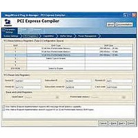
... For this walkthrough, specify pex for the name of the MegaCore function files: c:\altera\pcie_project\pex.vhd Figure 2–3 shows the MegaWizard Plug-In Manager after you have made these settings. PCI Express Compiler Version 6.1 Altera Corporation December 2006 ...
Page 27
... Getting Started 7. Parameterize To parameterize your MegaCore function, follow these steps: 1. Altera Corporation December 2006 Click Next to display the Parameter Settings page for the PCI Express Compiler (see Figure 2–4). 1 You can change the page that the MegaWizard Plug-In Manager displays by clicking Next or Back at the bottom of the dialog box ...
Page 28
... See the “BFM Test Driver Module For Simple DMA Example Design” on page 5–20 settings the test module uses. PCI Express Compiler Version 6.1 Table 2–1 BAR Size 16 MBytes - 24 bits 256 Kbytes -18 bits for a description of what Altera Corporation December 2006 ...
Page 29
... Getting Started 2. 3. Figure 2–5. Capabilities Page Altera Corporation December 2006 See “Parameter Settings” on page 3–31 of the available parameters. Click Next to display the Capabilities page. With the Capabilities page open, make the appropriate settings and click Next to display the Buffer Setup page. See PCI Express Compiler Version 6 ...
Page 30
... PCI Express Compiler User Guide The Buffer Setup page opens. Make the appropriate settings and click Next. See Figure 2–6. Table 3–20 on page Table 3–2 on page PCI Express Compiler Version 6.1 3–38. For additional information 3–15. Altera Corporation December 2006 ...
Page 31
... An IP functional simulation model is a cycle-accurate VHDL or Verilog HDL model produced by the Quartus II software. The model allows for fast functional simulation of IP using industry-standard VHDL and Verilog HDL simulators. Altera Corporation December 2006 The Power Management page opens. Make the appropriate settings. See Figure 2– ...
Page 32
... Using these models for synthesis will create a nonfunctional design. Click the Simulation Model tab (see Click the checkbox to enable the Generate Simulation Model (see Figure 2–8). Choose the language in the Language list pulldown. PCI Express Compiler Version 6.1 Figure 2–8). Altera Corporation December 2006 ...
Page 33
... Getting Started 4. Figure 2–9. Summary Generate Files To generate the files, follow these steps: 1. Altera Corporation December 2006 Click Next (or the Summary tab) to display the summary page (see Figure 2–9). Turn on the files you wish to generate.Use the check boxes on the Summary page to enable or disable the generation of specified files. ...
Page 34
... Pin Planner. This XML file is a Pin Planner support file that Pin Planner automatically uses. This file must remain in the same directory as the pex.ppf file. MegaCore function report file. PCI Express Compiler Version 6.1 Description Altera Corporation December 2006 ...
Page 35
... DMA example design. The directory also includes scripts for running the testbench in the ModelSim simulator. See Testbench & Example Designs created for the testbench. Altera Corporation December 2006 (Part This file instantiates the <variation name>_core module (or entity) that is described elsewhere in this ...
Page 36
... Verilog HDL IP functional simulation models. Design f For more information on IP functional simulation models, refer to the Simulating Altera IP in Third-Party Simulation Tools chapter in volume 3 of the Quartus II Development Software Handbook. IP Functional Simulation Model To run the testbench in the ModelSim simulator, follow these steps: 1 ...
Page 37
... These messages reflect the values entered during the parameterize step of the walkthrough. 1 Altera also provides the DOS command window batch file runtb.bat and the shell script runtb.sh to run the testbench in ModelSim command-line mode. Chapter 5, Testbench & Example “ ...
Page 38
... After you purchase a license for the PCI Express MegaCore function, you can request a license file from the Altera website at www.altera.com/licensing and install it on your computer. When you request a license file, Altera emails you a license.dat file. If you do not have Internet access, contact your local Altera representative. 2–16 ...
Page 39
... The PCI Express MegaCore functions comply with the PCI Express Base Specification 1.1 or the PCI Express Base Specification Revision 1.0a, and implements all three layers of the specification: ■ ■ Altera Corporation December 2006 broadly describes the roles of each layer of the PCI Express The data link layer ensures packet ...
Page 40
... Endpoint Types The MegaCore function can implement either a native PCI Express endpoint or a legacy endpoint. Altera recommends using native PCI Express endpoints for new applications; they support memory space read and write transactions only. Legacy endpoints provide compatibility with existing applications and can support I/O space read and write transactions ...
Page 41
... Rx0 Sequencing & Reordering Virtual Channel 1 Rx1 Data Rx1 Descriptor Rx1 Control & Status Rx1 Sequencing & Reordering Altera Corporation December 2006 Interface Established per Component Flow Control Check & Reordering Virtual Channel Arbitration & Tx Sequencing Flow Control Check & Reordering Receive Buffer Posted & ...
Page 42
... The transaction layer packet is forwarded by the application layer, the transaction layer arbitrates among virtual channels, and then forwards the priority transaction layer packet to the data link layer. PCI Express Compiler Version 6.1 Altera Corporation December 2006 ...
Page 43
... PCI Express™ Base Specification Revision 1.0a. f See in the PCI Express Base Specification 1.1 or the PCI Express Base Specification Revision 1.0a for the complete content of these registers. Altera Corporation December 2006 “Buffer Setup Page” on page Type 0 Configuration Space PCI Power Management Capability Structure ...
Page 44
... The MegaCore function can generate and transmit power management, interrupt, and error signaling messages automatically under the control of dedicated signals. Additionally, the MegaCore function can generate MSI requests under the control of the dedicated signals. PCI Express Compiler Version 6.1 Altera Corporation December 2006 ...
Page 45
... Figure 3–3 Altera Corporation December 2006 Link management through the reception and transmission of data link layer packets, which are used: To initialize and update flow control credits for each virtual ● channel For power management of data link layer packet reception and ● ...
Page 46
... CRC and maintains the integrity of transmitted packets. PCI Express Compiler Version 6.1 Towards Physical Layer Tx Packets Transmit Tx Arbitration Data Path Control & Status Data Link Control & Management State Machine Receive Data Path Rx Packets Altera Corporation December 2006 ...
Page 47
... Altera Corporation December 2006 Transaction Layer Packet Generator—This block generates transmit packets according to the descriptor and data received from the transaction layer, generating a sequence number and a 32-bit CRC. The packets are also sent to the retry buffer for internal storage. In ...
Page 48
... LTSSM PIPE State Machine Emulation Logic 8B/10B Decoder Rx MAC Lane 8B/10B Decoder Rx MAC Lane PCI Express Compiler Version 6.1 Towards Link PHY layer Tx+ / Tx- Transmit Data Path Tx+ / Tx- Rx+ / Rx- Elastic Buffer Receive Data Path Rx+ / Rx- Elastic Buffer Altera Corporation December 2006 ...
Page 49
... Writes consumes the data as quickly as possible, then the Flow Control Update loop can be the biggest determining factor in Write throughput, besides the actual bandwidth of the link. Altera Corporation December 2006 Media Access Controller (MAC) Layer—The MAC layer includes the link training and status state machine and the scrambling/descrambling and multilane deskew functions. PHY Layer— ...
Page 50
... PCI Express Compiler User Guide 3–5, Flow Control Update Loop, shows the main components of Figure Write Requester Write Completer Posted Headers Posted Data Non-Posted Headers Non-Posted Data Completion Headers Completion Data PCI Express Compiler Version 6.1 3–5, you see two communicating Altera Corporation December 2006 ...
Page 51
... Layer Data Source The following numbered steps describe each step in the Flow Control Update loop. The corresponding numbers on the diagram above show the general area to which they correspond Altera Corporation December 2006 FC FC Update DLLP DLLP Decode 6 Data Packet PCI Physical ...
Page 52
... TLP to complete before it can be sent. The FC Update DLLP is received back at the original Write Requester and the Credit Limit value is updated. If there were packets stalled waiting for credits, they now can be transmitted. PCI Express Compiler Version 6.1 Altera Corporation December 2006 ...
Page 53
... MegaCore function and Stratix II GX delays at both ends of the PCI Express Link. Some devices at the other end of the link could have smaller or larger delays, which would affect the minimum number of credits Altera Corporation December 2006 3–1, “FC Update Loop Delay Components For Stratix II GX,” shows ...
Page 54
... Logic. However, the delay differences are probably small compared with the inaccuracy in guessing what the external Read to Completion delays are. 3–16 PCI Express Compiler User Guide “Throughput of Posted Writes” on page PCI Express Compiler Version 6.1 3–11. The Altera Corporation December 2006 ...
Page 55
... Therefore, issuing eight (tag limit) 512 Byte read requests consumes 256 data credits, which is enough to keep the Read Request loop full and maximize the throughput. Altera Corporation December 2006 Table 3–3 shows the estimated completion space ...
Page 56
... Altera Corporation December 2006 ...
Page 57
... Reserved 0x00 0x00 Table 3–6 Table 3–6. MSI Capability Structure 31:24 23:16 Message Control Message Address Message Upper Address Reserved Altera Corporation December 2006 describes the type 0 configuration settings. 15:8 Vendor ID Command Revision ID 0x00 Cache Line Size Subsystem Vendor ID Capabilities PTR Int ...
Page 58
... PCI Express capability structure. 15:8 Next Cap PTR Capability ID Device control Link control Slot Control Root Control PCI Express Compiler Version 6.1 7:0 Byte Offset 078h 07Ch 7:0 Byte Offset 080h 084h 088h 08Ch 090h 094h 098h 09Ch 0A0h Altera Corporation December 2006 ...
Page 59
... Correctable Error Status Register Correctable Error Mask Register Advanced Error Capabilities and Control Register Header Log Register Root Error Command Root Error Status Error Source Identification Register Altera Corporation December 2006 describes the virtual channel capability structure. 15:8 Vers. Extended Cap ID Port VC Cap 1 VC arbit ...
Page 60
... Receive PLL—Receive PLLs train on the reference clock. When a lane exits electrical idle, each receive PLL synchronizes on the receive data (clock data recovery operation). If receive data has been generated on the reference clock of the slot, and if each receive PLL PCI Express Compiler Version 6.1 Altera Corporation December 2006 ...
Page 61
... Software compares the link exit latency with the endpoint’s acceptable latency to determine whether the component is permitted to use a particular power state. Altera Corporation December 2006 trains on this same reference clock, the synchronization time of the receive PLL is lower than if the reference clock is not the same for both components. Table 3– ...
Page 62
... L1 exit latency is 4 µs, and the endpoint acceptable latency is 2 µs, the exact L1 exit latency of the link will be 4 µs and software will probably not enable the entry to L1. To maximize performance, Altera recommends that you set L0s and L1 acceptable latency values to their minimum values. 3–12. ...
Page 63
... Correctable Replay Num Correctable Rollover Data Link Layer Uncorrectable Protocol (fatal) Altera Corporation December 2006 describes errors detected by the physical layer. Description This error has three potential causes: ● Physical coding sublayer error when a lane state. The error is reported per lane on ...
Page 64
... This error is caused by an unexpected completion transaction, either input from the application layer via the cpl_err[2] requestor ID does not match the endpoint's configured ID. PCI Express Compiler Version 6.1 rx_desc and rx_data busses cpl_err[0] cpl_err[1] signal when signal or when the Altera Corporation December 2006 ...
Page 65
... Error Logging & Reporting How the endpoint handles a particular error depends on the configuration registers of the device. error signaling and logging for an endpoint. Altera Corporation December 2006 Description This error occurs when a component receives a transaction layer packet that violates the FC credits allocated for this type of transaction layer packet ...
Page 66
... PCI Express Compiler Version 6.1 Yes Set correctable error detected bit in device status register. Set corresponding bit in correctable error status register. Masked in correctable error mask register? No Correctable error reporting enabled in device control register? Yes Send ERR_CORR Message End Altera Corporation December 2006 ...
Page 67
... Stratix GX devices do not exhibit the correct receiver impedance characteristics when the receiver input is at electrical idle. Stratix GX devices were designed before the PCI Express specification was Altera Corporation December 2006 Received poisoned transaction layer packets are sent to the application layer and status bits are automatically updated in the configuration space ...
Page 68
... This disables the PCI Express link preventing additional data transfer. The PCI Express capability registers in the configuration space are held in a reset state. PCI Express Compiler Version 6.1 and AN 320: OpenCore Plus Altera Corporation December 2006 ...
Page 69
... Settings System Settings Page The first page of the MegaWizard interface contains the parameters for the overall system settings and the base address registers. See Figure 3–7. System Settings Page Altera Corporation December 2006 PCI Express Compiler Version 6.1 Figure 3–7. 3–31 ...
Page 70
... Specifies the maximum number of lanes supported. The x8 value is supported only for a Stratix II GX PHY. Specifies the port type. Altera recommends Native endpoint for all new designs. Select Legacy Endpoint only when you require I/O transaction support for compatibility. See more information ...
Page 71
... BAR. The x1 and x4 MegaCore functions in Legacy Endpoint mode support I/O Space BARs sized from 16 Bytes to 4 KBytes. The x8 MegaCore function only supports I/O Space BARs of 4 KBytes. Altera Corporation December 2006 Value Displays a dialog box that allows you to configure the transceiver block ...
Page 72
... PCI Express link use the same clock source. There can be no PPM difference between the clocks at each end. PCI Express Compiler Version 6.1 Description Altera Corporation December 2006 ...
Page 73
... Vendor ID 16-bit Hex Class code 24-bit Hex Revision ID 8-bit Hex Altera Corporation December 2006 describes the parameters that you can set on this page. Description Sets the read-only value of the device ID register. Sets the read-only value of the vendor ID register. This parameter can not be set to 0xFFFF per the PCI Express Specification. ...
Page 74
... INTx Interrupt signals” on page 3–82 information. Indicates whether the MSI capability message control register is 64- bit addressing capable. PCI Express native endpoints always support MSI 64-bit addressing. PCI Express Compiler Version 6.1 for more Altera Corporation December 2006 ...
Page 75
... Specifications Buffer Setup Page The Buffer Setup page contains the parameters for the receive and retry buffers. See Figure 3–10. Buffer Setup Page Altera Corporation December 2006 Figure 3–10. PCI Express Compiler Version 6.1 3–37 PCI Express Compiler User Guide ...
Page 76
... Controls automatic configuration of the retry buffer based on the maximum payload size. Set the size of the retry buffer for storing transmitted PCI Express packets until acknowledged. Set the maximum number of packets that can be stored in the retry buffer. PCI Express Compiler Version 6.1 Altera Corporation December 2006 ...
Page 77
... Table 3–20. Buffer Setup Page Parameters (Part Parameter Value Desired performance Low, Medium, for received requests High, Maximum Altera Corporation December 2006 Description Specify how to configure the Rx Buffer size and the flow control credits. ● Low—Provides the minimal amount of space for desired traffic. ...
Page 78
... However, infinite completion credits are advertised on the PCI Express link as is required for endpoints the application layer to manage the rate of non-posted requests made to ensure that the Rx Buffer completion space does not overflow. PCI Express Compiler Version 6.1 “Analyzing Altera Corporation December 2006 ...
Page 79
... Power Management Page The Power Management page contains the parameters for setting various power management properties of the MegaCore function. See Figure Figure 3–11. Power Management Page Altera Corporation December 2006 3–11. PCI Express Compiler Version 6.1 3–41 PCI Express Compiler User Guide ...
Page 80
... Indicate the endpoint L1 acceptable latency. Sets the read- only value of the endpoint L1 acceptable latency field of the device capabilities register. This value should be based on how much latency the application layer can tolerate. PCI Express Compiler Version 6.1 Description Altera Corporation December 2006 ...
Page 81
... Figure 3–12 Transmit and receive signals apply to each implemented virtual channel, while configuration and global signals are common to all virtual channels on a link. Altera Corporation December 2006 Value Indicate the L1 exit latency for the separate clock. Used to calculate the value of the L1 exit latency field of the device capabilities register ...
Page 82
... Serial 16-Bit PIPE for x1 and x4 (Repeated for Lanes the x4 MegaCore Function) 8-Bit PIPE for x8 (Repeated for Lanes the x8 MegaCore Function) is changed to clk250_in for a x8 MegaCore function is changed to clk250_out for the x8 MegaCore function to test_out[127:0] for the x8 MegaCore function. Altera Corporation December 2006 ...
Page 83
... Transmit data path signals can be divided into two groups: ■ ■ 1 Altera Corporation December 2006 Descriptor Phase signals Data Phase signals In the following tables, transmit interface signal names suffixed with 0 are for virtual channel 0. If the MegaCore function implements additional virtual channels, there are an additional set of signals suffixed with the virtual channel number ...
Page 84
... The first DWORD is located on bits . set to 0: transaction layer packet without data set to 1: transaction layer packet with data signal. On the following clock cycle, a new tx_req . tx_desc PCI Express Compiler Version 6.1 is tx_ack . tx_data signal (kept tx_req Altera Corporation December 2006 ...
Page 85
... If the MegaCore function is not ready to acknowledge a descriptor phase (through assertion of transmission.When Altera Corporation December 2006 describes the standard data phase signals. Description to request a data phase (assuming a data phase is needed). This signal signal is valid ...
Page 86
... The first DWORD is located on bits . (32-bit address) set to 1: The first DWORD is located on bits . Clock Cycles Clock Cycles describes the advanced data phase signals. PCI Express Compiler Version 6.1 signal). directly to a tx_data[63:0] Altera Corporation December 2006 ...
Page 87
... If unused, this signal can be tied to zero. This signal is not available in the x8 MegaCore function. Notes for Table 3–24 (1) where n is the virtual channel number; For x1 and x4, n can (2) For x8, n can Altera Corporation December 2006 Description Table 3–25 for the bit detail. . ...
Page 88
... Maximum Payload Size. Ignore this field if value of the Posted Data credits, tx_cred[61] Non-Posted Header Ignore this field if value of the Non-Posted Header credits, PCI Express Compiler Version 6.1 Description Description , are set tx_cred[60] , set to 1. tx_cred[62] , set to 1. Altera Corporation December 2006 ...
Page 89
... In each waveform, a strong horizontal line separates descriptor signals from data signals. Altera Corporation December 2006 Value Non-Posted Data Ignore this field if value of the Non-Posted Data credits, Completion Header Completion Data: Posted Data: 9 bits permit advertisement of 256 credits, which corresponds to 4KB, the Maximum Payload Size ...
Page 90
... Descriptor tx_ack Signals tx_desc[127:0] tx_dfr tx_dv tx_data[63:32] Data Signals tx_data[31:0] tx_ws tx_err 3–52 PCI Express Compiler User Guide Clock Cycles CPLD X DW1 DW3 DW5 DW7 X DW0 DW2 DW4 DW6 PCI Express Compiler Version 6.1 Figure 3–13. The Altera Corporation December 2006 ...
Page 91
... Figure 3–14. Transfer for A Single DWORD Write 1 2 tx_req Descriptor tx_ack Signals tx_desc[127:0] tx_dfr tx_dv X tx _data[63:32] Data Signals tx_data[31:0] X tx_ws tx_err Altera Corporation December 2006 shows the MegaCore function transmitting a memory write Clock Cycles MEMWR32 DW0 PCI Express Compiler Version 6 ...
Page 92
... Figure 3–15. State Machine Is Busy with the Preceding Transaction Layer Packet Waveform 1 tx_req Descriptor tx_ack Signals tx_desc[127:0] tx_dfr tx_dv tx_data[63:32] Data Signals tx_data[31:0] tx_ws tx_err 3–54 PCI Express Compiler User Guide Clock Cycles MEMRD64 PCI Express Compiler Version 6.1 Figure 3–15 Altera Corporation December 2006 ...
Page 93
... MegaCore function is not configured with the maximum possible number of lanes implemented. Figure 3–17 asserting the wait state signal. Altera Corporation December 2006 shows that the application layer must wait to receive an Clock Cycles 3 ...
Page 94
... Descriptor tx_ack Signals tx_desc[127:0] tx_dfr tx_dv tx_data[63:32] Data Signals tx_data[31:0] tx_ws tx_err 3–56 PCI Express Compiler User Guide Clock Cycles MEMWR32 DW0 Clock Cycles MEMW32 X DW1 DW3 DW5 X DW0 DW2 DW4 PCI Express Compiler Version 6 DW7 X DW6 X Altera Corporation December 2006 ...
Page 95
... In this case, Figure 3–19. Inserting Wait States because of 4-DWORD Header Waveform 1 tx_req Descriptor tx_ack Signals tx_desc[127:0] tx_dfr tx_dv tx_data[63:32] Data Signals tx_data[31:0] tx_ws tx_err Altera Corporation December 2006 could have been sent one clock cycle later. tx_dv Clock Cycles MEMWR64 X DW0 ...
Page 96
... Signals tx_desc[127:0] tx_dfr tx_dv tx_data[63:32] Data Signals tx_data[31:0] tx_ws tx_err 3–58 PCI Express Compiler User Guide Figure 3–20. Clock Cycles MEMWR64 X DW1 DW3 X DW0 DW2 PCI Express Compiler Version 6.1 a second time to tx_ws DW5 DW7 X DW4 DW6 X Altera Corporation December 2006 ...
Page 97
... LCRC. This situation leads to an extra clock cycle between two consecutive transaction layer packets. Figure 3–21. 64-Bit Memory Read Request Waveform 1 tx_req Descriptor tx_ack Signals tx_desc[127:0] tx_dfr tx_dv tx_data[63:32] Data Signals tx_data[31:0] tx_ws tx_err Altera Corporation December 2006 Figure 3–21. Clock Cycles MEMRD64 MEMWR64 X DW1 ...
Page 98
... Data Signals tx_data[31:0] tx_ws tx_err 3–60 PCI Express Compiler User Guide Clock Cycles MEMWR64 X DW1 DW3 DW5 DW7 X DW0 DW2 DW4 DW6 PCI Express Compiler Version 6.1 Figure 3–22. No wait states are DW9 DW11 X DW8 DW10 X Altera Corporation December 2006 ...
Page 99
... Bits 126 and 127 indicate the transaction layer packet group and bits 135:128 describe BAR and address decoding information (see rx_desc[135:0] below for details). Receive Data Path Signals Receive data path signals can be divided into two groups: ■ ■ Altera Corporation December 2006 Clock Cycles ...
Page 100
... X Valid X X Valid X rx_desc[63:0] X Valid X set to 0: transaction layer packet without data rx_desc[126] rx_desc[126] set to 1: transaction layer packet with data PCI Express Compiler Version 6 and rx_abort rx_retry rx_ack for the Table 3–28. Completion rx_req 6 Altera Corporation December 2006 ...
Page 101
... For x1 and x4, n can (2) For x8, n can The MegaCore function generates the eight MSBs of this signal with BAR decoding information. See Table 3–28. rx_desc[135:128]: Descriptor & BAR Decoding Altera Corporation December 2006 Description signal is deasserted on the following clock cycle and rx_req is ready for the next transmission ...
Page 102
... The first DWORD is located on bits . (64-bit address) set to 1: The first DWORD is located on bits . (32-bit address) set to 1: The first DWORD is located on bits . Clock Cycles Clock Cycles PCI Express Compiler Version 6.1 . Each bit of rx_data[63:0] rx_data[63:0] directly to a 64-bit rx_data[63:0] Altera Corporation December 2006 ...
Page 103
... In each waveform, a strong horizontal line separates descriptor signals from data signals. Altera Corporation December 2006 Description Transaction without data payload Retried transaction and masked non-posted transactions Transaction aborted Transaction with data payload Transaction with data payload and wait states PCI Express Compiler Version 6.1 3– ...
Page 104
... MegaCore function receives three consecutive Memory read request (64-bit addressing mode) Memory read request (32-bit addressing mode) I/O read request Clock Cycles Valid X Valid MEMRD64 X MEMRD32 X Valid X Valid PCI Express Compiler Version 6 Valid X I Valid X Altera Corporation December 2006 ...
Page 105
... This update happens in clock cycles 8 and 12 in Altera Corporation December 2006 Between traffic classes mapped in the same virtual channel Between posted and completion transactions ...
Page 106
... PCI Express Compiler User Guide Clock Cycles Valid X Valid X MEMRD 4DW X MEMWR 1DW X Valid X Valid 00h F0h 3–26, a memory read of 16 DWORDS is sent to the application PCI Express Compiler Version 6 Valid X X MEMRD 4DW X X Valid X X 00h Altera Corporation December 2006 ...
Page 107
... In clock cycle 6, rx_abort is asserted and transmission of the next transaction begins on clock cycle 8. Figure 3–26. Aborted Transaction Waveform rx_req rx_ack rx_desc[135:128] rx_desc[127:64] Descriptor Signals rx_desc[63:0] rx_abort rx_retry rx_mask rx_dfr rx_dv rx_ws Data Signals rx_data[63:32] rx_data[31:0] rx_be[7:0] Altera Corporation December 2006 Clock Cycles Valid MEMRD 16DW X CPL 3DW Valid PCI Express Compiler Version 6 ...
Page 108
... Signals rx_data[63:32] rx_data[31:0] rx_be[7:0] 3–70 PCI Express Compiler User Guide 3–27, the MegaCore function receives a completion transaction Clock Cycles Valid X X CPLD 8DW X MEMWR AD1 3DW X Valid FFh PCI Express Compiler Version 6 Valid X X Valid F0h FFh X Altera Corporation December 2006 ...
Page 109
... Data Signals rx_data[63:32] rx_data[31:0] rx_be[7:0] Altera Corporation December 2006 The MegaCore function asserts rx_dv at clock cycle 10, thereby ending a MegaCore function-induced wait state. The application layer deasserts rx_ws at clock cycle 11, thereby ending an application interface-induced wait state. Clock Cycles 1 2 ...
Page 110
... Clocking The Altera PCI Express MegaCore functions use one of several possible clocking configurations, depending on the PHY (generic PIPE or Stratix GX) and the reference clock frequency. The functions have two clock input signals, refclk and clk125_in. The functions also have an output clock, clk125_out, that is a 125-MHz transceiver clock ...
Page 111
... You must connect clk125_out back to the clk125_in input, for example, through a distribution circuit needed in the application. All of the function’s interfaces, including the user application interface and the PIPE interface, are synchronous to the clk125_in input. See Figure Altera Corporation December 2006 3–29. altpcie_64b_x4_pipen1b: External PHY Not Required ...
Page 112
... Stratix GX 100 MHz 100-MHz refclk PLL 100 -> 125 clk125_in Figure 3–30: User and PIPE interface signals are synchronous to clk125_in. 3–31. PCI Express Compiler Version 6.1 (1) clk125_out ALTGXB Transceiver inclk rx_cruclk tx_coreclk All Logic in MegaCore Function clk Altera Corporation December 2006 ...
Page 113
... You must connect clk125_out back to the clk125_in input, for example, through a distribution circuit needed in the application. All of the function’s interfaces, including the user application interface and the PIPE interface, are synchronous to the clk125_in input. See Figure Altera Corporation December 2006 altpcie_64b_x4_pipen1b: Stratix GX 125 MHz 125-MHz refclk ...
Page 114
... Clock Source clk125_in Figure 3–32: User and PIPE interface signals are synchronous to clk125_in. for this clocking configuration. PCI Express Compiler Version 6.1 (1) ALTGXB Transceiver inclk coreclk_out clk125_out rx_cruclk tx_coreclk All Logic in MegaCore Function clk Figure 3–34 Altera Corporation December 2006 ...
Page 115
... The clk250_out must be connected back to the clk250_in input, possibly through any distribution circuit needed in the specific application. All of the interfaces of the function, including the user application interface and the PIPE interface are synchronous to the clk250_in input. See on page 3–78 Altera Corporation December 2006 altpcie_64b_x4_pipen1b: Stratix II GX (or x1) 100-MHz refclk ...
Page 116
... PIPE PHY device typically drives pclk . This signal is not on the x8 MegaCore function. input in Stratix GX PHY implementations. In generic PIPE PHY input drives this signal. This signal is not on the x8 refclk PCI Express Compiler Version 6.1 clk250_out signal directly. Altera Corporation December 2006 ...
Page 117
... DL up exit. This signal indicates the transition from DL_UP to DL_DOWN another dlup_exit source of internal reset and should cause the assertion of the synchronous resets. This signal is active low. Figure 3–35 Altera Corporation December 2006 Description , and ) are synchronous to this clock signal. This signal ...
Page 118
... Other Power On Reset perst# PCI Express Compiler Version 6.1 npor PCI Express MegaCore Function srst crst l2_exit hotrst_exit dlup_exit is not included as part of the npor PCI Express x8 MegaCore Function rstn l2_exit hotrst_exit dlup_exit Altera Corporation December 2006 ...
Page 119
... Power management turn off control register. This signal is asserted to pme_to_cr acknowledge the root port. O Power management turn off status register. This signal is asserted when the pme_to_sr endpoint receives the until Altera Corporation December 2006 Figure 3–36 shows the function’s power management signals. Description message by sending PME_turn_off PME_turn_off is asserted. ...
Page 120
... PME_EN : Reserved : PM_STATE illustrates the behavior of pme_to_sr and pme_to_cr in an Clock Cycles PCI Express Compiler Version 6 PME_EN Data_select PM_state Reserved signal independent of the PME# : This field indicates the scaling factor : This field indicates which data should Altera Corporation December 2006 ...
Page 121
... Configuration MSI control status register. This bus provides MSI software control. cfg_msicsr[15:0] ● ● ● ● ● ● Altera Corporation December 2006 describes MegaCore function’s interrupt signals. Description : Reserved. cfg_msicsr[15:9] : Per vector masking capable cfg_msicsr[8] 1: function supports MSI per vector masking ...
Page 122
... Description INT# message is generated and the status is register. int_status illustrates the architecture of the MSI handler block. app_msi_req app_msi_ack app_msi_tc app_msi_num pex_msi_num app_int_sts cfg_msicsr[31:0] illustrates a possible implementation of the MSI handler PCI Express Compiler Version 6.1 MSI Handler Block Altera Corporation December 2006 ...
Page 123
... For example, in eight MSI but is only allocated two. In this case, the application layer must be designed to use only two allocated messages. Figure 3–40. MSI Request Example Altera Corporation December 2006 app_int_sts app_int_en0 app_msi_req0 ...
Page 124
... PCI Express Compiler User Guide illustrates the interactions among MSI interrupt signals for Figure 3–40. The minimum latency possible between Clock Cycles Valid Valid describes 3 example implementations; one in which all 32 MSI MSI PCI Express Compiler Version 6 Allocated 29:0 1:0 2:0 Altera Corporation December 2006 ...
Page 125
... O Configuration dev control status register. See PCI Express specification for details. cfg_devcsr[31:0] O Configuration link control status register. See PCI Express specification for details. cfg_linkcsr[31:0] Altera Corporation December 2006 Table 3–35 reflect the current values of several Description cfg_tcvcmap[2:0] : Mapping for TC0 (always 0). ...
Page 126
... PCI Express Compiler User Guide shows the function’s completion interface signals. Description : This signal must be asserted when a cpl_err[0] cpl_err[1] : This signal must be asserted when a target cpl_err[2] PCI Express Compiler Version 6.1 : This signal must be asserted when a Altera Corporation December 2006 ...
Page 127
... The following signals exist: ■ ■ ■ ■ Table 3–38 Altera Corporation December 2006 shows the maximum completion space signals. Description This static signal reflects the amount of Rx Buffer space reserved for completion headers and data. It provides the same information as what is shown in the Rx buffer space allocation table of the wizard’ ...
Page 128
... ALT2GXB dynamic reconfiguration clock. reconfig_togxb[2:0] input bus is the ALT2GXB dynamic reconfiguration output signal is the ALT2GXB dynamic reconfiguration reconfig_fromgxb PCI Express Compiler Version 6.1 Figure 3–12 on page 3–44 for a Altera Corporation December 2006 ...
Page 129
... Setting 1-bit interface. When simulating, you can set this signal to indicate which interface is used for the simulation. When compiling your design for an Altera device, set this signal to 0. PIPE Interface Signals The x1 and x4 MegaCore function is compliant with the 16-bit version of the PIPE interface, enabling use of an external PHY ...
Page 130
... Receive status 0: This signal encodes receive status and error codes for the receive data stream and receiver detection. PCI Express Compiler Version 6.1 and the second . For the x8 MegaCore for the first for the second (8b/10b and the second is is available. is available. . Altera Corporation December 2006 ...
Page 131
... Altera Corporation December 2006 Description Asynchronous reset to external phy tied high and expects a pull-down resistor on the board. During FPGA configuration, the pull-down resistor will reset the phy and after that the FPGA will drive the phy out of reset. ...
Page 132
... Compatibility Testing Environment Altera has performed significant hardware testing of the PCI Express MegaCore functions to ensure a reliable solution. The MegaCore functions have been tested at various PCI-SIGs PCI Express Compliance Workshops in 2005 and 2006 with Stratix II GX and various external PHYs, and they have passed all PCI-SIG gold tests and interoperability tests with a wide selection of motherboards and test equipment ...
Page 133
... PHY is included in the <variation name> module or entity. The user logic must instantiate this module or entity in his design. The implementation details for each of these modes are discussed in the following sections. Altera Corporation December 2006 Clock Frequency 125 MHz In this generic 16-bit PIPE interface, both the ...
Page 134
... PLL source file to set the required phase shift. Then add the modified PLL source file to your Quartus II project. tlp_clk62p5 is a 62.5 MHz output that drives the tlp_clk input of the MegaCore function when the MegaCore internal clock frequency is 62.5 MHz. PCI Express Compiler Version 6.1 4–1. The clk125_in is used to Altera Corporation December 2006 ...
Page 135
... SDR Mode with a Source Synchronous TxClk The implementation of the 16-bit SDR mode with a source synchronous TxClk is shown in <variation name>.v or <variation name>.vhd. In this mode the following clocking scheme is used: ■ ■ ■ Altera Corporation December 2006 125Mhz SDR Mode without txclk rxdata ...
Page 136
... DDR register that is used to create a center aligned TxClk. 125Mhz 16-bit SDR Mode with txclk tlp_clk @ 125Mhz ENB ENB ENB DDIO ENB PCI Express Compiler Version 6.1 Figure 4–1, PCIe IP MegaCore clk125_in tlp_clk refclk clk125_out Altera Corporation December 2006 ...
Page 137
... An edge detect circuit is used to detect the relationships between the 125 MHz clock and the 250 MHz rising edge to properly sequence the 16-bit data into the 8-bit output register. Altera Corporation December 2006 A zero delay copy of the 125 MHz refclk. The zero delay PLL output is used as the clk125_in for the core and clocks a double data rate register for the incoming receive data ...
Page 138
... A zero delay copy of the 125 MHz refclk used as the clk125_in for the MegaCore function and also to clock DDR input registers for the Rx data and status signals. PCI Express Compiler Version 6.1 clk125_in Tlp_clkt PCIe IP MegaCore txdata_h txdata_l refclk clk125_out Altera Corporation December 2006 ...
Page 139
... Mode 3 txdata txclk External connection in user logic Altera Corporation December 2006 A 250 MHz "early" clock PLL output clocks an 8-bit SDR transmit data output register. This 250 MHz early output is multiplied from the 125 MHz refclk and is early in relation to the refclk. A 250 MHz single data rate register for the 125 MHz DDR output allows you to use the SDR output registers in the Cyclone II IOB ...
Page 140
... II software to edit the PLL source file to set the required phase shift. Then add the modified PLL source file to your Quartus II project. An optional 62.5 MHz TLP Slow clock is provided for x1 implementations. PCI Express Compiler Version 6.1 Figure 4–5 and is Altera Corporation December 2006 ...
Page 141
... The implementation of the 16-bit SDR mode with a source synchronous TxClk is shown in <variation name>.v or <variation name>.vhd and includes a PLL. The PLL inclock is driven by refclk (pclk from the external PHY) and has the following 3 outputs: ■ ■ Altera Corporation December 2006 250Mhz SDR Mode ...
Page 142
... PCI Express Compiler User Guide An optional 62.5 MHz TLP Slow clock is provided for x1 implementations ENB ENB ENB ENB tlp_clk clk125_zero PCI Express Compiler Version 6 rxdata_h Q 4 ENB Q 1 rxdata_l Q 4 ENB clk125_in PCIe IP MegaCore txdata_h txdata_l tlp_clk refclk Altera Corporation December 2006 ...
Page 143
... O rxdata1_ext[15:0] I rxdatak1_ext[1:0] I rxelecidle1_ext I rxpolarity1_ext O Altera Corporation December 2006 Table 4–2. Depending on the number of lanes selected and Description PCI Express Reset signal, active low. PIPE Interface phystatus signal. PHY is signaling completion of the requested operation PIPE Interface powerdown signal, requests the PHY to enter the specified power state. ...
Page 144
... Only in x4 Only in x4 Only in x4 Only in x4 Only in x4 Only in x4 Only in x4 Only in x4 Only in x4 Only in x4 Only in x4 Only in x4 Only in x4 Only in x4 Only in x4 Only in x4 Only in x4 Only in x4 Only in x4 Altera Corporation December 2006 ...
Page 145
... I rxelecidle1_ext I rxpolarity1_ext O rxstatus1_ext[1:0] I rxvalid1_ext I Altera Corporation December 2006 Table 4–3. Depending on the number of lanes selected and Description PCI Express Reset signal, active low. PIPE Interface phystatus signal. PHY is signaling completion of the requested operation PIPE Interface powerdown signal, requests the PHY to enter the specified power state. ...
Page 146
... Only in x4 Only in x4 Only in x4 Only in x4 Only in x4 Only in x4 Only in x4 Only in x4 Only in x4 Only in x4 Only in x4 Only in x4 Only in x4 Only in x4 Only in x4 Only in x4 Only in x4 Only in x4 Only in x4 Altera Corporation December 2006 ...
Page 147
... By selecting the Custom option, you can select any of the supported interfaces. the external PHY. Figure 4–7. Selecting an External PHY During Parameterization Altera Corporation December 2006 Select the exact PHY Select the type of interface to the PHY. Several PHYs have multiple interface modes. ...
Page 148
... The TI XIO1100 device has some additional control signals that need to be driven by your design. These can be statically pulled high or low in the board design, unless additional flexibility is needed by your design and you want to drive them from the Altera device. These signals are: ■ ■ ...
Page 149
... If you are using the Stratix GX internal PHY this is not necessary. To modify the PLL instance, follow these steps Altera Corporation December 2006 Copy the PLL source file referenced in your variation file from the <path>/ip/PCI Express Compiler/lib directory to your project directory. Use the MegaWizard Plug In Manger in the Quartus II software to edit the PLL to use the Stratix GX device family ...
Page 150
... External PHY Constraint Support 4–18 PCI Express Compiler User Guide PCI Express Compiler Version 6.1 Altera Corporation December 2006 ...
Page 151
... PCI Express link monitoring and error injection capabilities are limited to those provided by the MegaCore function’s test_in and test_out signals. The following sections describe the testbench, two example designs, and root BFM in detail. Altera Corporation December 2006 A simple DMA example design A chaining DMA example design 2– ...
Page 152
... The Altera testbench and root port BFM provide a simple method to do basic testing of the application layer logic that interfaces to the MegaCore function endpoint variation. However, the testbench and root port BFM are not intended substitute for a full verification environment. To thoroughly test your application, Altera suggests that you obtain commercially available PCI Express verification IP and tools, and/or do your own extensive hardware testing ...
Page 153
... Figure 5–1. Testbench Top-Level Module: <variation name>_testbench Testbench Top Level (<variation name>_testbench) Endpoint Example Design <variation name>_example_pipen1b The top-level of the testbench instantiates four main modules: ■ ■ ■ Altera Corporation December 2006 Figure 5–1 PIPE Interconnection Module (x8) (altpcierd_pipe_phy) Chaining DMA Test Driver Module (altpcietb_bfm_driver_chaining) < ...
Page 154
... MegaCore function operate faster than specified in the PCI Express specification.This should usually be set to 1, but can be set there is a need to simulate the true time-out values. PCI Express Compiler Version 6.1 “BFM Test 5–20. Description (PIPE_MODE = used for the (PIPE_MODE = 0 Altera Corporation December 2006 ...
Page 155
... The example endpoint design can be used in the testbench simulation and to compile a complete design for an Altera device. All of the modules necessary to implement the example design with the variation file are contained in separate files, based on the language you use: <variation name>_example_top.vhd < ...
Page 156
... I/Os. These test ports can be used in your design. PCI Express Compiler Version 6.1 for more information. PHY Support Module (< variation name >) PCI Express MegaCore Function Variation Appendix C) which allows you to Altera Corporation December 2006 ...
Page 157
... Testbench & Example Designs ■ ■ ■ ■ ■ Altera Corporation December 2006 <variation name>.vhd or <variation name>.v— This file instantiates the <variation name>_core entity (or module) that is described elsewhere in this section and includes additional logic required to support the specific PHY you have chosen for your variation ...
Page 158
... Writing the PCI Express address to the registers at offset 0x00 and 0x04. Writing the master memory block address to the register at offset 0x14. Writing the length of the requested operation to the register at offset 0x08. PCI Express Compiler Version 6.1 Table 5–3 Example Design Control Altera Corporation December 2006 ...
Page 159
... Sets value of the EP bit in all PCI Express request headers generated by this DMA channel operation. The EP bit is the poisoned data bit. Altera Corporation December 2006 Writing the attributes (including PCI Express memory write or read direction) of the requested operation to the register at offset 0x0C. ...
Page 160
... PCI Express address. 5–10 PCI Express Compiler User Guide Description 00b—Memory read (3DW w/o data) 01b—Memory read (4DW w/o data) 10b—Memory write (3DW w/data) 11b—Memory write (4DW w/data) PCI Express Compiler Version 6.1 Altera Corporation December 2006 ...
Page 161
... RC memory to EP memory. The chaining DMA example design endpoint design is completely contained within a supported Altera device and relies on no other hardware interface than the PCI Express link. This allows you to use the example design for the initial hardware validation of your system. ...
Page 162
... Two Root Complex (RC) memory descriptor tables, one for each DMA module. These are described in the following section CPU and associated PCI Express PHY link to the EP example design, using a Root Port and a North/South Bridge. PCI Express Compiler Version 6.1 Altera Corporation December 2006 ...
Page 163
... You can use the example endpoint design in the testbench simulation and compile a complete design for an Altera device. All of the modules necessary to implement the example design with the variation file are contained in one of the following files, based on the language you use: < ...
Page 164
... RC Slave module for performance monitoring and single ● DWORD Mrd/Mwr Header Register module: RC programs the descriptor header (4 ● DWORDS) at the beginning of the DMA PCI Express Compiler Version 6.1 Appendix C, ) which allows you to Altera Corporation December 2006 ...
Page 165
... Port) to retrieve the DMA Performance counter values and performs single DWORD read and write to the Endpoint memory by bypassing the DMA engine. By default, this module is disabled. Altera Corporation December 2006 Descriptor module: DMA engine collects chaining descriptors ● ...
Page 166
... Writing to this register starts the execution of the DMA channel operation. Reading the DMA channel operation in progress bit at offset 0x0C to determine when the DMA channel operation has completed. PCI Express Compiler Version 6.1 Altera Corporation December 2006 ...
Page 167
... Header Field Access Access Size R R/W Direction R R/W Message R R/W Signaled Interrupt (MSI) Altera Corporation December 2006 Tables 5–5, 5–6, and , describe each of the fields of this 5–6) BDT Upper DWORD BDT Lower DWORD MSI Number Reserved EPLAST_ENA MSI EP Address 0x00 (DMA write) ...
Page 168
... DMA transfer status. 0x0C (DMA write) RCLAST reflects the number of descriptors ready to 0x1C (DMA read) be transferred. Your software application can periodically update this register based on system level memory scheduling constraints. PCI Express Compiler Version 6.1 Description [4:0]. [2:0} Altera Corporation December 2006 ...
Page 169
... RC Address R Lower DWORD DMA Length R EPLAST_ENA R MSI R Altera Corporation December 2006 Table 5–8 for the format of the descriptor fields following the Table describes each descriptor field. 5–8, 5–9, are related to the list of descriptor tables which resides 22 21 Control Fields (see Table ...
Page 170
... Sets up a 4,096 byte data pattern in the BFM shared memory, which is done by a call to the shemem_fill procedure in altpcietb_bfm_shmem. b. Writes those 4,096 bytes to the example endpoint design target memory, which is done by a call to the ebfm_barwr procedure in altpcietb_bfm_rdwr. PCI Express Compiler Version 6.1 Altera Corporation December 2006 ...
Page 171
... Testbench & Example Designs 4. 5. Altera Corporation December 2006 c. Reads the same 4,096 bytes from the target memory to a separate location in the BFM shared memory, which is done by a call to the ebfm_barrd_wait procedure in altpcietb_bfm_rdwr. This procedure blocks (waits) until the completion has been received for the read. ...
Page 172
... The test next checks that each MSI is received before the watchdog timer expires, and that the MSI data received is correct. d. Restores the MSI control register to the pre-test state, and reports the results of the test. PCI Express Compiler Version 6.1 Altera Corporation December 2006 ...
Page 173
... DMA Write Cycles The procedure dma_wr_test used for DMA writes uses the following steps: 1. Altera Corporation December 2006 e. The simulation is stopped by calling the procedure ebfm_log_stop_sim in altpcieb_bfm_log. Configures the root port and endpoint configuration spaces, which the BFM test driver module does by calling the procedure ebfm_cfg_rp_ep, which is part of altpcierd_bfm_configure ...
Page 174
... BFM shared memory upper address value 0x04800 BFM shared memory lower address value Increment from Data content in the BFM shared memory from 0xCCC0_FFFF address: 0x04800 0x4860 PCI Express Compiler Version 6.1 Description Description Table on page 5–19) Description Altera Corporation December 2006 ...
Page 175
... The procedure dma_rd_test used for DMA reads uses the following three steps Altera Corporation December 2006 Set up the chaining DMA descriptor header and starts the transfer data from the EP memory to the BFM shared memory. This is done by a call to the procedure dma_set_header which writes the ...
Page 176
... BFM shared memory lower address value Increment from Data content in the BFM shared memory from 0xCCC0_FFFF address: 0x20900 0x20960 PCI Express Compiler Version 6.1 Description Table on page 5–19) Description Table on page 5–19) Description Table on page 5–19) Altera Corporation December 2006 ...
Page 177
... BFM Shared Memory (altpcietb_bfm_shmem) BFM Log Interface (altpcietb_bfm_log) Root Port RTL Model (altpcietb_bfm_rp_top_x8_pipen1b) IP Functional Simulation (altpcietb_bfm_rpvar_64b_x8_pipen1b) The root port BFM consists of these main components: ■ Altera Corporation December 2006 Figure 5–4 BFM Read/Write Shared Request Procedures (altpcietb_bfm_rdwr) (altpcietb_bfm_configure) BFM Request Interface (altpcietb_bfm_req_intf) ...
Page 178
... Root Port RTL Model (altpcietb_bfm_rp_top_x8_pipen1b VHDL entity or Verilog HDL Module) — This is the Register Transfer Level (RTL) portion of the model. This takes the requests from the above PCI Express Compiler Version 6.1 5–42. 5–44. “BFM Log 5–50. Altera Corporation December 2006 ...
Page 179
... The specified bus number is assigned to be the secondary bus in the root port configuration space. Altera Corporation December 2006 modules and handles them at an RTL level to interface to the PCI Express link. You do not need to access this module directly to adapt the testbench to test your endpoint application. VC0:3 Interfaces (altpcietb_bfm_vc_intf) — ...
Page 180
... Sets the endpoint Max Read Request Size equal to the Max Payload Size since the root port does not support breaking the read request into multiple completions. PCI Express Compiler Version 6.1 Altera Corporation December 2006 ...
Page 181
... Testbench & Example Designs 3. Altera Corporation December 2006 Assigns values to all the endpoint BAR registers. The BAR addresses are assigned by the algorithm outlined below. a. I/O BARs are assigned smallest to largest starting just above the ending address of BFM shared memory in I/O space and continuing as needed throughout a full 32-bit I/O space ...
Page 182
... VC interface module for transmission. ebfm_barwr_imm —writes a maximum of four bytes of immediate data (passed in a procedure call offset from a specific endpoint BAR. This procedure returns as soon as the request has been passed to the VC interface module for transmission. PCI Express Compiler Version 6.1 Altera Corporation December 2006 ...
Page 183
... HDL tasks to allow these functions to be called by other Verilog HDL functions. Unless explicitly specified otherwise, all procedures in the following sections also are implemented as Verilog HDL tasks. 1 Altera Corporation December 2006 ebfm_barrd_wait — reads data from an offset of a specific endpoint BAR and stores it in BFM shared memory. This procedure blocks waiting for the completion data to be returned before returning control to the caller ...
Page 184
... Length, in bytes, of the data written. Can the minimum of the bytes byte_len remaining in the BAR space or BFM shared memory Traffic class used for the PCI Express transaction tclass 5–34 PCI Express Compiler User Guide pcie_offset PCI Express Compiler Version 6.1 to determine PCI Express address Altera Corporation December 2006 ...
Page 185
... Syntax ebfm_barwr_imm(bar_table, bar_num, pcie_offset, imm_data, byte_len, tclass) Arguments bar_table bar_num pcie_offset imm_data byte_len tclass Altera Corporation December 2006 Address of the endpoint bar_table memory Number of the BAR used with pcie_offset Express address Address offset from the BAR base Data to be written. In VHDL, this argument is a std_logic_vector(31 downto 0). ...
Page 186
... BFM shared memory address where the read data is stored Length, in bytes, of the data to be read. Can the minimum of the bytes remaining in the BAR space or BFM shared memory Traffic class used for the PCI Express transaction PCI Express Compiler Version 6.1 to determine PCI Altera Corporation December 2006 ...
Page 187
... Arguments bar_table bar_num pcie_offset lcladdr byte_len tclass Altera Corporation December 2006 Address of the endpoint bar_table Number of the BAR used with pcie_offset address Address offset from the BAR base BFM shared memory address where the read data is stored Length, in bytes, of the data to be read ...
Page 188
... In both languages, this argument is the completion status as specified in the PCI Express specification: compl_status Definition 000 SC —Successful completion 001 UR —Unsupported Request 010 CRS —Configuration Request Retry Status 100 CA —Completer Abort PCI Express Compiler Version 6.1 (2 downto 0) and is set by Altera Corporation December 2006 ...
Page 189
... Data to be written imm_data In VHDL. this argument is a std_logic_vector(31 downto 0). In Verilog HDL, this argument is reg [31:0]. In both languages, the bits written depend on the length: Length Altera Corporation December 2006 arguments cannot cross a DWORD boundary. Bits Written 4 31 downto downto 0 ...
Page 190
... In Verilog HDL, this argument is reg [2:0]. In both languages, this is the completion status as specified in the PCI Express specification: compl_status Definition 000 SC —Successful completion 001 UR —Unsupported Request 010 CRS —Configuration Request Retry Status 100 CA —Completer Abort PCI Express Compiler Version 6.1 (2 downto 0) and is set Altera Corporation December 2006 ...
Page 191
... The above counters are continuously counting from the start of simulation. The procedure ebfm_start_perf_sample resets all of the counters to 0. Altera Corporation December 2006 PCI Express bus number of the target device PCI Express bus number of the target device PCI Express device number of the target device ...
Page 192
... This procedure simply resets the performance counters. The procedure waits until the next Root Port BFM clock edge to ensure the counters are synchronously reset. Calling this routine effectively starts a performance sampling window. 5–42 PCI Express Compiler User Guide PCI Express Compiler Version 6.1 Altera Corporation December 2006 ...
Page 193
... INFO: 92850 ns PERF: # INFO: 92850 ns PERF: # INFO: 92850 ns PERF: The above example is from a VHDL version of the testbench. The Verilog version may have slightly different formatting. Altera Corporation December 2006 Tx Packets MByte/sec: 1767 Tx Mbit/sec: 14134 Rx Packets MByte/sec: 1764 Rx Mbit/sec: 14109 PCI Express Compiler Version 6.1 ...
Page 194
... All Verilog HDL arguments are type INTEGER and are input-only unless specified otherwise. 5–44 PCI Express Compiler User Guide describes the information in Description PCI Express Compiler Version 6.1 Figure 5–5: e was last called. Tx Bytes divided by Tx MByte/sec Altera Corporation December 2006 ...
Page 195
... Arguments bar_table ep_bus_num ep_dev_num rp_max_rd_req_size display_ep_config addr_map_4GB_limit Altera Corporation December 2006 Address of the endpoint bar_table memory. The bar_table structure is populated by this routine. PCI Express bus number of the target device. This can be any value greater than 0. The root port is configured to use this as it’s secondary bus number ...
Page 196
... All Verilog HDL arguments are type INTEGER and are input-only unless specified otherwise. 5–46 PCI Express Compiler User Guide argument is set by the procedure to indicate if the BAR is a std_logic argument is set by the procedure to indicate if the BAR is a std_logic PCI Express Compiler Version 6.1 Altera Corporation December 2006 ...
Page 197
... Table 5–30. shmem_write VHDL Procedure or Verilog HDL Task Syntax shmem_write(addr, data, leng) Arguments addr data leng Altera Corporation December 2006 Description BFM shared memory starting address for writing data Data to write to BFM shared memory. In VHDL, this argument is an unconstrained vector must be 8 times the long ...
Page 198
... Should be on the constants defined in 5–48 PCI Express Compiler User Guide std_logic_vector is less than 8 bytes, only the corresponding least leng PCI Express Compiler Version 6 which the vector is 8 times addr ; bits 15 for more information on Table 5–35 on page 5–52. Altera Corporation December 2006 ...
Page 199
... Arguments addr mode leng init Altera Corporation December 2006 BFM shared memory starting address for filling data Data pattern used for filling the data. Should be one of the constants defined in section “Shared Memory Constants” on page Length, in bytes, of data to fill. If the length is not a multiple of the incrementing data pattern width, then the last data pattern is truncated to fit ...
Page 200
... FALSE—Data pattern did not compare successfully Result in Verilog HDL is 1-bit. 1’b1 — Data patterns compared successfully 1’b0 — Data patterns did not compare successfully PCI Express Compiler Version 6.1 “Shared Memory Constants” on std_logic_vector(63 downto . reg [63:0] Altera Corporation December 2006 ...