CDB42L52 Cirrus Logic Inc, CDB42L52 Datasheet - Page 3
CDB42L52
Manufacturer Part Number
CDB42L52
Description
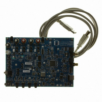
Eval Bd LP Codec W/Class D Spkr Driver
Manufacturer
Cirrus Logic Inc
Specifications of CDB42L52
Main Purpose
Audio, CODEC
Embedded
Yes, FPGA / CPLD
Utilized Ic / Part
CS42L52
Primary Attributes
4 Stereo Audio Inputs, Stereo Line and Speaker Outputs, S/PDIF Inputs and Outputs
Secondary Attributes
GUI, I2C, SPI, USB Interfaces
Description/function
Audio CODECs
Operating Supply Voltage
5 V
Product
Audio Modules
Lead Free Status / RoHS Status
Contains lead / RoHS non-compliant
For Use With/related Products
CS42L52
Lead Free Status / RoHS Status
Contains lead / RoHS non-compliant
Other names
598-1505


DS680DB1
1. SYSTEM OVERVIEW
The CDB42L52 platform provides analog and digital interfaces to the CS42L52 and allows for external DSP and
I²C
sary. Board configuration is done using the Windows PC-compatible GUI to read/write device registers. An FPGA
on the board helps make clock/data routing and CS42L52 configuration easy.
The CDB42L52 schematic set has been partitioned into seven pages and is shown in
tem Connections and Jumpers” on page 13
the default factory settings for all jumpers.
ration details.
1.1
1.2
1.3
1.4
WARNING: Please refer to the CS42L52 data sheet for allowable voltage levels.
®
interconnect. On board power regulators are provided so that only an external +5 V power supply is neces-
Power
Power is supplied to the evaluation board via the USB connection or by applying +5.0 V to TP2. Jumper J34
allows the user to select the power source. Power (VP) and ground (GND) for the PWM output stages in the
CS42L52 is supplied via binding posts J35 and J4 (respectively) or by standard AAA batteries in locations
BT1, BT2 and BT3. The VP voltage level can be in the range of +1.6 V to +5.25 V. On board regulators and
jumpers allow the user to connect the CODEC’s supplies to +1.65 V, 2.5 V or +3.3 V for VL and +1.65 V or
2.5 V for VD, VA and VA_HP. All voltage inputs must be referenced to ground using the black binding post
J4.
Stake headers/Jumpers and parallel resistors provide a convenient way to measure supply currents to the
CS42L52 for VD, VA, VL, VA_HP and VP supplies. The current is easily calculated by measuring the volt-
age drop across this resistor with its associated jumper removed. NOTE: The stake headers connected in
parallel with these resistors must be shunted with the supplied jumper during normal operation.
Grounding and Power Supply Decoupling
The CS42L52 requires careful attention to power supply and grounding arrangements to optimize perfor-
mance. The CDB42L52 demonstrates these optimal arrangements.
view of the connections to the CS42L52.
on page 22
pling capacitors are located as close as possible to the CS42L52. Extensive use of ground plane fill helps
reduce radiated noise.
FPGA
The FPGA controls digital signal routing between the CS42L52, CS8406, CS8416, SRC, PLL and the I/O
stake header. It also provides routing control of the system master clock from an on-board oscillator, the
CS8416 and the I/O stake header. The Cirrus FlexGUI software provides full control of the FPGA’s routing
and configuration options.
CS42L52 Audio CODEC
A complete description of the CS42L52
sheet.
The CS42L52 is configured using the Cirrus FlexGUI. The device configuration registers are accessible via
the “Register Maps” tab of the Cirrus FlexGUI software. This tab provides low-level control of each bit. For
easier configuration, additional tabs provide high-level control.
page 6
provides configuration details.
shows the top layout, and
Section 2. “Software Mode Control” on page 6
Section 2. “Software Mode Control” on page 6
provides a description of all stake headers and connectors, including
Figure 16 on page 25
(Figure 4 on page
Figure 12 on page 21
17) can be found in the CS42L52 product data
shows the bottom layout. Power supply decou-
shows the component placement,
Section 2. “Software Mode Control” on
Figure 7 on page 16
provides configuration details.
Figures 4
provides further configu-
through 11.
provides an over-
CDB42L52
Figure 13
“Sys-
3
Related parts for CDB42L52
Image
Part Number
Description
Manufacturer
Datasheet
Request
R

Part Number:
Description:
Development Kit
Manufacturer:
Cirrus Logic Inc
Datasheet:
Part Number:
Description:
Development Kit
Manufacturer:
Cirrus Logic Inc
Datasheet:


Part Number:
Description:
High-efficiency PFC + Fluorescent Lamp Driver Reference Design
Manufacturer:
Cirrus Logic Inc
Datasheet:
Part Number:
Description:
Development Kit
Manufacturer:
Cirrus Logic Inc
Datasheet:
Part Number:
Description:
Development Kit
Manufacturer:
Cirrus Logic Inc
Datasheet:

Part Number:
Description:
Development Kit
Manufacturer:
Cirrus Logic Inc
Datasheet:
Part Number:
Description:
Development Kit
Manufacturer:
Cirrus Logic Inc
Datasheet:
Part Number:
Description:
Development Kit
Manufacturer:
Cirrus Logic Inc
Datasheet:
Part Number:
Description:
Development Kit
Manufacturer:
Cirrus Logic Inc
Datasheet:

Part Number:
Description:
EVALUATION BOARD FOR CS8427
Manufacturer:
Cirrus Logic Inc
Datasheet:

Part Number:
Description:
BOARD EVAL FOR CS8416 RCVR
Manufacturer:
Cirrus Logic Inc
Datasheet:

Part Number:
Description:
EVALUATION BOARD FOR CS8420
Manufacturer:
Cirrus Logic Inc
Datasheet:

Part Number:
Description:
KIT DEVELOPMENT EP9315 ARM9
Manufacturer:
Cirrus Logic Inc
Datasheet:

Part Number:
Description:
KIT DEVELOPMENT EP9302 ARM9
Manufacturer:
Cirrus Logic Inc
Datasheet: