CDB42L52 Cirrus Logic Inc, CDB42L52 Datasheet
CDB42L52
Specifications of CDB42L52


Related parts for CDB42L52


CDB42L52 Summary of contents
Page 1
Low-power, Stereo CODEC w/ Headphone & Speaker Amps Stereo CODEC High Performance Stereo ADC & DAC – (ADC (DAC) Dyn. Range (A-wtd) – -88 dB THD+N Flexible Stereo Analog Input Architecture – 4:1 Analog Input MUX ...
Page 2
System Features 12, 24, and 27 MHz Master Clock Support in Addition to Typical Audio Clock Rates High-performance 24-bit Converters – Multi-bit Delta-Sigma Architecture – Very Low 64Fs Oversampling Clock Reduces Power Consumption Low-power Operation – Stereo Analog Passthrough: 10 ...
Page 3
TABLE OF CONTENTS 1. PIN DESCRIPTIONS .............................................................................................................................. 8 1.1 I/O Pin Characteristics ...................................................................................................................... 9 2. TYPICAL CONNECTION DIAGRAM ................................................................................................... 10 3. CHARACTERISTIC AND SPECIFICATIONS ...................................................................................... 11 RECOMMENDED OPERATING CONDITIONS ................................................................................... 11 ABSOLUTE MAXIMUM RATINGS ....................................................................................................... 11 ANALOG INPUT CHARACTERISTICS (COMMERCIAL ...
Page 4
I²C Control ........................................................................................................................... 38 4.12.2 Memory Address Pointer (MAP) .......................................................................................... 39 4.12.2.1 Map Increment (INCR) ............................................................................................. 39 5. REGISTER QUICK REFERENCE ........................................................................................................ 40 6. REGISTER DESCRIPTION .................................................................................................................. 42 6.1 Chip I.D. and Revision Register (Address 01h) (Read Only) ......................................................... ...
Page 5
Invert ADC Signal Polarity ................................................................................................... 51 6.11.5 ADC Mute ............................................................................................................................ 51 6.12 Playback Control 1 (Address 0Dh) ............................................................................................... 51 6.12.1 Headphone Analog Gain ..................................................................................................... 51 6.12.2 Playback Volume Setting B=A ............................................................................................ 51 6.12.3 Invert PCM Signal Polarity .................................................................................................. 52 ...
Page 6
Bass Gain ............................................................................................................................ 63 6.25 Master Volume Control: MSTA (Address 20h) & MSTB (Address 21h) ....................................... 63 6.25.1 Master Volume Control ........................................................................................................ 63 6.26 Headphone Volume Control: HPA (Address 22h) & HPB (Address 23h) ..................................... 63 6.26.1 Headphone Volume ...
Page 7
Auto Detect Disabled ...................................................................................................................... 76 9. PCB LAYOUT CONSIDERATIONS ..................................................................................................... 77 9.1 Power Supply, Grounding ............................................................................................................... 77 9.2 QFN Thermal Pad .......................................................................................................................... 77 10. ADC & DAC DIGITAL FILTERS ........................................................................................................ 78 11. PARAMETER DEFINITIONS .............................................................................................................. 79 12. PACKAGE DIMENSIONS ...
Page 8
PIN DESCRIPTIONS SDA 1 SCL 2 AD0 3 SPKR_OUTA SPKR_OUTA- 6 SPKR_OUTB SPKR_OUTB- 9 -VHPFILT 10 Pin Name # SDA 1 Serial Control Data (Input/Output) - SDA is a data I/O in I²C ...
Page 9
AGND 17 Analog Ground (Input) - Ground reference for the internal analog section. Positive Voltage Reference (Output) - Positive reference voltage for the internal sampling cir- FILT+ 18 cuits Quiescent Voltage (Output) - Filter connection for the internal ...
Page 10
TYPICAL CONNECTION DIAGRAM +1 +2 *Use low ESR ceramic capacitors. Digital Audio Processor Ω +1 +3.3 V Notes: 1. Recommended values for the default charge pump switching frequency. The required capacitance ...
Page 11
CHARACTERISTIC AND SPECIFICATIONS RECOMMENDED OPERATING CONDITIONS AGND=DGND=0 V, All voltages with respect to ground. Parameters DC Power Supply Analog Headphone Amplifier Speaker Amplifier Digital Serial/Control Port Interface Ambient Temperature ABSOLUTE MAXIMUM RATINGS AGND = DGND = 0 V; All ...
Page 12
ANALOG INPUT CHARACTERISTICS (COMMERCIAL - CNZ) Test Conditions (unless otherwise specified): Input sine wave (relative to digital full scale): 1 kHz through passive input filter; All Supplies = VA +25°C; Sample Frequency = 48 kHz; Measurement Bandwidth is ...
Page 13
ANALOG INPUT CHARACTERISTICS (AUTOMOTIVE - DNZ) otherwise specified): Input sine wave (relative to full-scale): 1 kHz through passive input filter; All Supplies = VA; T +85°C; Sample Frequency = 48 kHz; Measurement Bandwidth kHz unless ...
Page 14
ADC DIGITAL FILTER CHARACTERISTICS Parameters Passband (Frequency Response) Passband Ripple Stopband Stopband Attenuation Total Group Delay High-Pass Filter Characteristics (48 kHz Fs) Frequency Response Phase Deviation @ 20 Hz Passband Ripple Filter Settling Time 5. Response is clock-dependent and will ...
Page 15
ANALOG OUTPUT CHARACTERISTICS (COMMERCIAL - CNZ) Test conditions (unless otherwise specified): Input test signal is a full-scale 997 Hz sine wave; All Supplies = VA; T Sample Frequency = 48 kHz; Measurement bandwidth kHz; Test ...
Page 16
ANALOG OUTPUT CHARACTERISTICS (AUTOMOTIVE - DNZ) Test conditions (unless otherwise specified): Input test signal is a full-scale 997 Hz sine wave; All Supplies = VA; T +85°C; Sample Frequency = 48 kHz and 96 kHz; Measurement bandwidth ...
Page 17
ANALOG PASSTHROUGH CHARACTERISTICS Test Conditions (unless otherwise specified): Input sine wave (relative to full-scale): 1 kHz through passive input filter; PGA and HP/Line Gain = 0 dB; All Supplies = VA; T “Required Initialization Settings” on page 37 Parameters Analog ...
Page 18
Parameters (Note 10 3.7 V Power Output per Channel Stereo Full-Bridge Mono Parallel Full-Bridge Total Harmonic Distortion + Noise Stereo Full-Bridge Mono Parallel Full-Bridge Dynamic Range Stereo Full-Bridge Mono Parallel Full-Bridge VP =2.5 V Power Output per Channel ...
Page 19
HEADPHONE OUTPUT POWER CHARACTERISTICS Test conditions (unless otherwise specified): Input test signal is a full-scale 997 Hz sine wave; Sample Frequency = 48 kHz; Measurement Bandwidth kHz; Test load R on page 37 written on ...
Page 20
LINE OUTPUT VOLTAGE LEVEL CHARACTERISTICS Test conditions (unless otherwise specified): Input test signal is a full-scale 997 Hz sine wave; measurement bandwidth kHz; Sample Frequency = 48 kHz; Test load R page 37 written on ...
Page 21
SWITCHING SPECIFICATIONS - SERIAL PORT Inputs: Logic 0 = DGND, Logic 1 = VL, SDOUT C Parameters RESET pin Low Pulse Width MCLK Frequency (Note 15) MCLK Duty Cycle Slave Mode Input Sample Rate (LRCK) LRCK Duty Cycle SCLK Frequency ...
Page 22
SWITCHING SPECIFICATIONS - I²C CONTROL PORT Inputs: Logic 0 = DGND, Logic 1 = VL, SDA C Parameters SCL Clock Frequency RESET Rising Edge to Start Bus Free Time Between Transmissions Start Condition Hold Time (prior to first clock pulse) ...
Page 23
DC ELECTRICAL CHARACTERISTICS AGND = 0 V; All voltages with respect to ground. Parameters VQ Characteristics Nominal Voltage Output Impedance DC Current Source/Sink MIC BIAS Characteristics Nominal Voltage DC Output Current Power Supply Rejection Ratio (PSRR) Power Supply Rejection Ratio ...
Page 24
POWER CONSUMPTION Operation Off (Note 21) 2 Standby (Note 22 Mono Record ADC ...
Page 25
APPLICATIONS 4.1 Overview 4.1.1 Basic Architecture The CS42L52 is a highly integrated, low-power, 24-bit audio CODEC comprised of a stereo analog-to- digital converter (ADC), a stereo digital-to-analog converter (DAC), a digital PWM modulator and two full- bridge power back-ends. ...
Page 26
Analog Inputs DIGSUM [1:0] ALCA ALCASRDIS ALCAZCDIS ALCARATE[5:0] ALCRRATE[5:0] Swap/ Mix MAX[2:0] M IN[2:0] DIGM IX ALCB ALCBSRDIS ALCBZCDIS Referenced Control Register Location Analog Front End PDN_PGAx ......................... “Power Down PGAx” on page 42 PGAxVOL[5:0]..................... “PGAx Volume” on page ...
Page 27
MIC Inputs The input pins 21, 22, 23, and 24 accept stereo line-level or microphone signals. For microphone inputs, either single-ended or differential configuration is allowed, providing programmable pre-amplification of low-level signals. In the single-ended configuration, an internal MUX ...
Page 28
Referenced Control Register Location PGAxVOL[5:0 “PGAx Vol. & ALCx Transition Ctl.: ALC, PGA A (Address 12h) & ALC, PGA B (Address 13h)” on ...
Page 29
Analog Outputs INPUTS FROM ADCA and ADCB AMIXAMUTE AMIXBMUTE AMIXAVOL[6:0] AMIXBVOL[6:0] +12dB/-51.5dB 0.5dB steps PMIXAMUTE PMIXBMUTE PMIXAVOL[6:0] PMIXBVOL[6:0] +12dB/-51.5dB 0.5dB steps Demph VOL DEEMPH INV_PCMA INV_PCMB OFFTIME[2:0] ONTIME[3:0] FREQ[3:0] BEEP[1:0] BEEPMIXDIS Generator Digital Mix to ADC Serial Interface Referenced ...
Page 30
BATTCMP VPREF[3:0] VPLVL[7:0] SPKAMUTE SPKBMUTE Battery MUTE50/50 SPKMONO Compensation SPKSWAP SPKB=A SPKAVOL[7:0] SPKBVOL[7:0] +0dB/-102dB 0.5dB steps PWM from DSP Gate VOL Modulator Engine Drive PDN_SPKA[1:0] PDN_SPKB[1:0] SPKASHRT SPKBSHRT Figure 11. PWM Output Stage Referenced Control Register Location PWM Control SPKxMUTE ...
Page 31
CONTINUOUS BEEP: Beep turns configurable frequency (FREQ) and volume (BPVOL) and remains on BEEP[1:0] = until BEEP is cleared. '11' MULTI-BEEP: Beep turns configurable frequency (FREQ) BEEP[1:0] = '10' and volume (BPVOL) for the ...
Page 32
ite fte ite 4.4 Analog In ...
Page 33
Referenced Control PDN_ADCx ......................... PASSTHRU ......................... PDN_OVRD ........................ SPKx_PDN[1:0]................... 4.4.2 Overriding the PGA Power Down To accommodate automatic activation of the headphone amplifier when the SPK/HP_SW switch pin changes, the CS42L52 will automatically power up the PGA whenever passthrough is ...
Page 34
Maintaining a Desired Output Level Using SPKxVOL, the speaker output level must first be attenuated by the decibel equivalent of the expect supply range (MAX relative to MIN). The CS42L52 then gradually reduces the attenuation as the ...
Page 35
MCLK Sample Rate, (MHz) Fs (kHz) 8.0000 12.0000 16.0000 12.2880 24.0000 32.0000 48.0000 96.0000 11.0250 22.0500 11.2896 44.1000 88.2000 8.0000 12.0000 18.4320 16.0000 (Slave 24.0000 Mode 32.0000 ONLY) 48.0000 96.0000 8.0182 16.9344 11.0250 (Slave 22.0500 Mode 44.1000 ONLY) 88.2000 8.0000 ...
Page 36
Digital Interface Formats The serial port operates in standard I²S, Left-justified, Right-justified (DAC only), or DSP Mode digital inter- face formats with varying bit depths from 16 to 24. Data is clocked out of the ADC or into the ...
Page 37
Initialization The CODEC enters a Power-down state upon initial power-up. The interpolation and decimation filters, del- ta-sigma and PWM modulators, and control port registers are reset. The internal voltage reference, and switched-capacitor low-pass filters are powered down. The device ...
Page 38
Control Port Operation The control port is used to access the registers, allowing the CODEC to be configured for the desired oper- ational modes and formats. The operation of the control port may be completely asynchronous with respect to ...
Page 39
Send start condition. Send 10010100 (chip address & write operation). Receive acknowledge bit. Send MAP byte, auto-increment off. Receive acknowledge bit. Send stop condition, aborting write. Send start condition. Send 10010101 (chip address & read operation). Receive acknowledge bit. Receive ...
Page 40
REGISTER QUICK REFERENCE Default values are shown below the bit names ( I²C Address : 1001010[R/W] - 10010100 = 0x94(Write); 10010101 = 0x95(Read) Adr. Function 7 01h ID CHIPID4 CHIPID3 02h Power Ctl 1 PDN_CHRG Reserved ...
Page 41
I²C Address : 1001010[R/W] - 10010100 = 0x94(Write); 10010101 = 0x95(Read) Adr. Function 7 1Bh PCMMIXB Vol PMIXBMUTE PMIXBVOL6 PMIXBVOL5 1Ch BEEP Freq, FREQ3 FREQ2 On Time 1Dh BEEP Vol, OFFTIME2 OFFTIME1 Off Time ...
Page 42
REGISTER DESCRIPTION All registers are read/write except for the chip I.D. and Revision Register and Interrupt Status Register which are read only. See the following bit definition tables for bit assignment information. The default state of each bit after ...
Page 43
The PGAxSEL bits may be used to isolate the input signal(s) from the PGA outputs. When the PGA is powered down, no input should be selected. Refer to “PGA Input Mapping” on page 49 6.2.3 Power Down ADCx ...
Page 44
Power Control 3 (Address 04h PDN_HPB1 PDN_HPB0 PDN_HPA1 6.4.1 Headphone Power Control Configures how the SPKR/HP pin, 31, controls the power for the headphone amplifier. PDN_HPx[1:0] Headphone Status Headphone channel is ON when the SPKR/HP pin, 31, ...
Page 45
Speed Mode Configures the speed mode of the CODEC in slave mode and sets the appropriate MCLK divide ratio for LRCK and SCLK in master mode. Slave Mode SPEED[1:0] Serial Port Speed 00 Double-Speed Mode (DSM - 50 kHz ...
Page 46
MCLK Divide By 2 Divides the input MCLK by 2 prior to all internal circuitry. MCLKDIV2 MCLK signal into CODEC 0 No divide 1 Divided by 2 Application: “Serial Port Clocking” on page 34 Note: In slave mode, this ...
Page 47
DAC Interface Format Configures the digital interface format for data on SDIN. DACDIF[1:0] DAC Interface Format 00 Left Justified 24-bit data 01 I² 24-bit data 10 Right Justified 11 Reserved Application: “Digital Interface Formats” on ...
Page 48
Tri-State Serial Port Interface Determines the state of the serial port drivers. Serial Port Status 3ST_SP Slave Mode 0 Serial Port clocks are inputs and SDOUT is output 1 Serial Port clocks are inputs and SDOUT is HI-Z Notes: ...
Page 49
PGA Input Mapping Selects one or sums/mixes the analog input signal into the PGA. Each bit of the PGAx_SEL[5:1] word corresponds to individual channels (i.e. PGAx_SEL1 selects AIN1x, PGAx_SEL2 selects AIN2x, etc.). PGAxSEL[5:1] Selected Input to PGAx (Examples) 00000 ...
Page 50
ADC HPF Corner Frequency (Address 0Bh Reserved Reserved Reserved 6.10.1 HPF x Corner Frequency Sets the corner frequency (-3 dB point) for the internal High-Pass Filter (HPF). HPFx_CF[1:0] HPF Corner Frequency Setting (Fs=48 kHz) 00 Normal setting ...
Page 51
Invert ADC Signal Polarity Configures the polarity of the ADC signal. INV_ADCx ADC Signal Polarity 0 Not Inverted 1 Inverted 6.11.5 ADC Mute Configures a digital mute on ADC channel x. ADCxMUTE ADC Mute 0 Disabled 1 Enabled Note: ...
Page 52
Invert PCM Signal Polarity Configures the polarity of the digital input signal. INV_PCMx PCM Signal Polarity 0 Not Inverted 1 Inverted 6.12.4 Master Playback Mute Configures a digital mute on the master volume control for channel x. MSTxMUTE Master ...
Page 53
HP/Speaker De-emphasis Configures a 15µs/50µs digital de-emphasis filter response on the headphone/line and speaker outputs DEEMPHASIS Control Port Status 0 Disabled 1 Enabled 6.13.5 Digital Soft Ramp Configures an incremental volume ramp from the current level to the new ...
Page 54
Playback Control 2 (Address 0Fh HPBMUTE HPAMUTE SPKBMUTE 6.14.1 Headphone Mute Configures a digital mute on headphone channel x. HPxMUTE Headphone Mute 0 Disabled 1 Enabled 6.14.2 Speaker Mute Configures a digital mute on speaker channel x. ...
Page 55
MICx Amp Control:MIC A (Address 10h) & MIC B (Address 11h Reserved MICxSEL MICxCFG 6.15.1 MIC x Select Selects one of two single-ended MIC inputs on channel x. MICxSEL MIC x Selection 0 MIC 1x 1 MIC ...
Page 56
ALCx Zero Cross Disable Configures an override of the analog zero cross setting. ALCxZCDIS ALC Zero Cross Disable 0 OFF; ALC Attack Rate is dictated by the ANLGZC 1 ON; ALC volume changes take effect at any time, regardless ...
Page 57
Passthrough x Volume: PASSAVOL (Address 14h) & PASSBVOL (Address 15h PASSxVOL7 PASSxVOL6 PASSxVOL5 6.17.1 Passthrough x Volume Sets the volume/gain of the signal routed from the PGA to the headphone/line output. PASSxVOL[7:0] Gain 0111 1111 12 dB ...
Page 58
ADCx Mixer Volume: ADCA (Address 18h) & ADCB (Address 19h AMIXxMUTE AMIXxVOL6 AMIXxVOL5 6.19.1 ADC Mixer Channel x Mute Configures a digital mute on the ADC mix in the DSP. AMIXxMUTE ADC Mixer Mute 0 Disabled 1 ...
Page 59
Beep Frequency & On Time (Address 1Ch FREQ3 FREQ2 FREQ1 6.21.1 Beep Frequency Sets the frequency of the beep signal. FREQ[3:0] Frequency (Fs = 12, 24 kHz) 0000 260.87 Hz 0001 521.74 Hz 0010 ...
Page 60
Beep On Time Sets the on duration of the beep signal. ONTIME[3:0] On Time (Fs = 12, 24 kHz) 0000 ~86 ms 0001 ~430 ms 0010 ~780 ms 0011 ~1.20 s 0100 ~1.50 s 0101 ~1.80 ...
Page 61
Beep Volume Sets the volume of the beep signal. BEEPVOL[4:0] Gain 00110 +6.0 dB ··· ··· 00000 -6 dB 11111 -8 dB 11110 -10 dB ··· ··· 00111 -56 dB Step Size Application: “Beep Generator” on page ...
Page 62
Treble Corner Frequency Sets the corner frequency (-3 dB point) for the treble shelving filter. TREBCF[1:0] Treble Corner Frequency Setting 00 5 kHz 01 7 kHz 10 10 kHz 11 15 kHz 6.23.4 Bass Corner Frequency Sets the corner ...
Page 63
Bass Gain Sets the gain of the bass shelving filter. TREB[3:0] Gain Setting 0000 +12.0 dB ··· ··· 0111 +1.5 dB 1000 0 dB 1001 -1.5 dB ··· ··· 1111 -10.5 dB Step Size: 1.5 dB 6.25 Master Volume ...
Page 64
Speaker Volume Control: SPKA (Address 24h) & SPKB (Address 25h SPKxVOL7 SPKxVOL6 SPKxVOL5 6.27.1 Speaker Volume Control Sets the volume of the signal out the PWM modulator. SPKxVOL[7:0] Speaker Volume 0000 0000 0 dB 1111 1111 -0.5 ...
Page 65
Limiter Control 1, Min/Max Thresholds (Address 27h LMAX2 LMAX1 LMAX0 6.29.1 Limiter Maximum Threshold Sets the maximum level, below full scale, at which to limit and attenuate the output signal at the attack rate (LIMARATE - “Limiter ...
Page 66
Limiter Zero Cross Disable Configures an override of the digital zero-cross setting. LIMZCDIS Limiter Zero Cross Disable 0 OFF; Limiter Attack Rate is dictated by the DIGZC 1 ON; Limiter volume changes take effect in one step, regardless of ...
Page 67
Limiter Attack Rate (Address 29h Reserved Reserved LIMARATE5 6.31.1 Limiter Attack Rate Sets the rate at which the limiter applies digital attenuation from levels above the MAX[2:0] threshold (“Limiter Maximum Threshold” on page LIMARATE[5:0] Attack Time 00 ...
Page 68
ALC Release Rate (Address 2Bh Reserved Reserved ALCRRATE5 6.33.1 ALC Release Rate Sets the rate at which the ALC releases the analog and/or digital attenuation from levels below the MIN[2:0] threshold (“ALC Minimum Threshold” on page VOL[5:0] ...
Page 69
ALC Minimum Threshold Sets the minimum level at which to disengage the ALC’s attenuation or amplify the input signal at the re- lease rate (ALCRRATE - CMIN thresholds. ALCMIN[2:0] Threshold Setting 000 0 dB 001 -3 dB 010 -6 ...
Page 70
Noise Gate Threshold and Boost THRESH sets the threshold level of the noise gate. Input signals below the threshold level will be attenu- ated to -96 dB. NG_BOOST configures a +30 dB boost to the threshold settings. THRESH[2:0] Minimum ...
Page 71
DSP Engine Overflow (Read Only) Indicates the over-range status in the DSP data path. DSPxOVFL DSP Overflow Status digital clipping has occurred in the data path after the DSP. 1 Digital clipping has occurred in the data ...
Page 72
VP Reference Sets the desired VP reference used for battery compensation. VPREF[3:0] Desired VP used to calculate the required attenuation on the speaker output: 0000 1.5 V 0001 2.0 V 0010 2.5 V 0011 3.0 V 0100 3.5 V ...
Page 73
SPKR/HP Pin Status (Read Only) Indicates the status of the SPKR/HP pin. SPKR/HP Pin State 0 Pulled Low 1 Pulled High 6.40 Charge Pump Frequency (Address 34h CHGFREQ3 CHGFREQ2 CHGFREQ1 6.40.1 Charge Pump Frequency Sets the charge ...
Page 74
ANALOG PERFORMANCE PLOTS 7.1 Headphone THD+N versus Output Power Plots Test conditions (unless otherwise specified): Input test signal is a 997 Hz sine wave; measurement band- width kHz kHz. -10 -15 ...
Page 75
VHP = VA = 1.8 V -20 -30 -35 -40 -45 - -65 -70 -75 -80 -85 -90 -95 -100 0 6m 12m 18m 24m Figure 24. THD+N vs. Output Power per Channel at ...
Page 76
EXAMPLE SYSTEM CLOCK FREQUENCIES 8.1 Auto Detect Enabled Sample Rate LRCK (kHz) 8 11.025 12 Sample Rate LRCK (kHz) 16 22.05 24 Sample Rate LRCK (kHz) 32 44.1 48 Sample Rate LRCK (kHz) 64 88.2 96 8.2 Auto Detect ...
Page 77
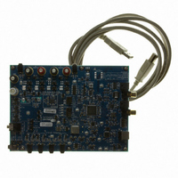
... All signals, especially clocks, should be kept away from the FILT+ and VQ pins in order to avoid unwanted coupling into the modulators. The FILT+ and VQ decoupling capacitors, particularly the 0.1 µF, must be po- sitioned to minimize the electrical path from FILT+ and AGND. The CDB42L52 evaluation board demon- strates the optimum layout and power supply arrangements. ...
Page 78
DAC DIGITAL FILTERS Figure 26. ADC Passband Ripple Figure 28. ADC Transition Band Figure 30. DAC Passband Ripple Figure 32. DAC Transition Band 78 5/13/08 Figure 27. ADC Stopband Rejection Figure 29. ADC Transition Band (Detail) Figure 31. ...
Page 79
DEFINITIONS Dynamic Range The ratio of the rms value of the signal to the rms sum of all other spectral components over the specified bandwidth. Dynamic Range is a signal-to-noise ratio measurement over the specified band width made with ...
Page 80
DIMENSIONS 40L QFN ( BODY) PACKAGE DRAWING D 2.00 REF PIN #1 IDENTIFIER ∅0.50±0.10 LASER MARKING INCHES DIM MIN 0.0000 b 0.0071 0.0091 D 0.2362 BSC D2 0.1594 0.1614 E 0.2362 BSC E2 ...
Page 81
... CS42L52 Container Order # Rail CS42L52-CNZ Tape & Reel CS42L52-CNZR Rail CS42L52-DNZ Tape & Reel CS42L52-DNZR - - CDB42L52 - - CRD42L52 9. 24. “Automatic Level Control (ALC)” on “Required Initialization Settings” on page “Analog Front-End Volume Setting B=A” on 54. “Beep Volume” on page 61. 37. ...
Page 82
Contacting Cirrus Logic Support For all product questions and inquiries, contact a Cirrus Logic Sales Representative. To find one nearest you www.cirrus.com. IMPORTANT NOTICE Cirrus Logic, Inc. and its subsidiaries (“Cirrus”) believe that the information contained in this ...