CDB42L52 Cirrus Logic Inc, CDB42L52 Datasheet - Page 24
CDB42L52
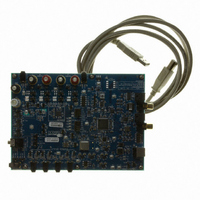
Manufacturer Part Number
CDB42L52
Description
Eval Bd LP Codec W/Class D Spkr Driver
Manufacturer
Cirrus Logic Inc
Specifications of CDB42L52
Main Purpose
Audio, CODEC
Embedded
Yes, FPGA / CPLD
Utilized Ic / Part
CS42L52
Primary Attributes
4 Stereo Audio Inputs, Stereo Line and Speaker Outputs, S/PDIF Inputs and Outputs
Secondary Attributes
GUI, I2C, SPI, USB Interfaces
Description/function
Audio CODECs
Operating Supply Voltage
5 V
Product
Audio Modules
Lead Free Status / RoHS Status
Contains lead / RoHS non-compliant
For Use With/related Products
CS42L52
Lead Free Status / RoHS Status
Contains lead / RoHS non-compliant
Other names
598-1505


24
POWER CONSUMPTION
1
2
3
4
5
6
7
8
9
10
11
12
13
Operation
Off
Standby
Mono Record
Stereo Record
Mono Playback to Headphone
Mono Playback to Speaker
Stereo Playback to Headphone
Stereo Playback to Speaker
Stereo Passthrough to Head-
phone
Mono Record & Playback
PGA in (no MIC) to Mono HP
Phone Monitor
MIC (w/bias) in to Mono Out
Stereo Record & Playback
PGA in (no MIC) to St. HP Out
Stereo Rec. & Full Playback
PGA (no MIC) to St. HP & SPK
(Note 21)
20. Unless otherwise noted, test conditions are as follows: All zeros input, slave mode, sample
21. RESET pin 25 held LO, all clocks and data lines are held LO.
22. RESET pin 25 held HI, all clocks and data lines are held HI.
23. VL current will slightly increase in master mode.
(Note 22)
rate = 48 kHz; No load. Digital (VD) and logic (VL) supply current will vary depending on speed mode
and master/slave operation.
MIC to PGA to ADC
MIC to PGA to ADC
MIC to PGA to ADC
PGA to ADC 1 0 1 0 0 1 1 1 11 11 11 11
PGA to ADC 0 0 0 0 0 1 1 1 11 11 11 11
(with Bias)
(no Bias)
(no Bias)
ADC 1 1 1 0 0 1 1 1 11 11 11 11
ADC 1 1 0 0 0 1 1 1 11 11 11 11
x x x x x x x x x
x x x x 1 x x x x
1 0 1 0 0 1 0 0 11 11 11 11
1 0 1 0 0 1 0 1 11 11 11 11
0 0 0 0 0 0 0 1 11 11 11 11
1 1 1 1 0 1 1 1 10 11 11 11
1 1 1 1 0 1 1 1 11 11 10 10
1 1 1 1 0 1 1 1 10 10 11 11
1 1 1 1 0 1 1 1 11 11 10 10
1 1 1 1 0 1 1 1 10 10 11 11
1 0 1 0 0 1 1 1 11 10 11 11
1 0 1 0 0 1 0 0 11 10 11 11
0 0 0 0 0 1 1 1 10 10 11 11
0 0 0 0 0 1 1 1 10 10 10 10
02h
See
Power Ctl. Registers
“Required Initialization Settings” on page 37
(Note
03h
20).
5/13/08
x
x
04h
x
x
x
x
1.8 0.00
2.5 0.00
1.8 0.00
2.5 0.00
1.8 0.00
2.5 0.00
1.8 0.00
2.5 0.00
1.8 0.00
2.5 0.00
1.8 0.00
2.5 0.00
1.8 0.00
2.5 0.00
1.8 0.00
2.5 0.00
1.8 0.00
2.5 0.00
1.8 1.59
2.5 2.07
1.8 0.00
2.5 0.00
1.8 2.77
2.5 3.27
1.8 0.00
2.5 0.00
1.8 2.79
2.5 3.18
1.8 1.77
2.5 2.13
1.8 1.76
2.5 2.15
1.8 2.76
2.5 3.21
1.8 3.49
2.5 3.95
V
i
VHP
0.00
0.00
0.00
0.00
1.67
1.87
3.48
3.71
3.15
3.37
2.31
2.53
3.18
3.42
5.32
5.57
1.99
2.62
0.20
0.22
2.00
2.63
0.20
0.22
1.91
2.14
3.95
4.77
5.33
6.19
5.05
5.90
5.24
6.10
Typical Current (mA)
2.1
2.3
i
VA
10.46
0.00
0.00
0.01
0.02
2.32
3.72
2.31
3.72
2.32
3.72
2.32
3.73
2.37
3.82
2.37
3.81
2.37
3.81
2.72
4.27
4.42
6.77
2.91
4.28
4.38
6.80
1.06
1.81
4.28
6.63
4.28
6.69
4.64
7.17
7.20
written on power up.
i
VD
(Note 23)
VL=3.3V
0.00
0.00
0.03
0.03
0.03
0.03
0.03
0.03
0.03
0.01
0.01
0.01
0.01
0.01
0.03
0.03
0.03
0.03
i
VL
VP=3.7V
0.00
0.00
0.00
0.00
0.00
0.00
0.00
0.00
0.00
0.00
1.00
0.00
1.00
0.00
0.00
0.00
0.00
1.00
i
CS42L52
VP
DS680F1
(mW
Power
14.05
15.13
10.49
18.65
17.83
15.95
10.04
18.15
13.90
23.53
11.36
22.43
12.05
21.21
13.84
25.48
11.98
21.28
10.39
17.85
18.05
33.90
20.52
37.65
22.46
40.78
32.47
55.07
Total
0.00
0.00
0.02
0.05
7.24
7.99
9.90
8.48
rms
)
Related parts for CDB42L52
Image
Part Number
Description
Manufacturer
Datasheet
Request
R

Part Number:
Description:
Development Kit
Manufacturer:
Cirrus Logic Inc
Datasheet:
Part Number:
Description:
Development Kit
Manufacturer:
Cirrus Logic Inc
Datasheet:


Part Number:
Description:
High-efficiency PFC + Fluorescent Lamp Driver Reference Design
Manufacturer:
Cirrus Logic Inc
Datasheet:
Part Number:
Description:
Development Kit
Manufacturer:
Cirrus Logic Inc
Datasheet:
Part Number:
Description:
Development Kit
Manufacturer:
Cirrus Logic Inc
Datasheet:

Part Number:
Description:
Development Kit
Manufacturer:
Cirrus Logic Inc
Datasheet:
Part Number:
Description:
Development Kit
Manufacturer:
Cirrus Logic Inc
Datasheet:
Part Number:
Description:
Development Kit
Manufacturer:
Cirrus Logic Inc
Datasheet:
Part Number:
Description:
Development Kit
Manufacturer:
Cirrus Logic Inc
Datasheet:

Part Number:
Description:
EVALUATION BOARD FOR CS8427
Manufacturer:
Cirrus Logic Inc
Datasheet:

Part Number:
Description:
BOARD EVAL FOR CS8416 RCVR
Manufacturer:
Cirrus Logic Inc
Datasheet:

Part Number:
Description:
EVALUATION BOARD FOR CS8420
Manufacturer:
Cirrus Logic Inc
Datasheet:

Part Number:
Description:
KIT DEVELOPMENT EP9315 ARM9
Manufacturer:
Cirrus Logic Inc
Datasheet:

Part Number:
Description:
KIT DEVELOPMENT EP9302 ARM9
Manufacturer:
Cirrus Logic Inc
Datasheet: