CDB42L52 Cirrus Logic Inc, CDB42L52 Datasheet - Page 37
CDB42L52
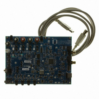
Manufacturer Part Number
CDB42L52
Description
Eval Bd LP Codec W/Class D Spkr Driver
Manufacturer
Cirrus Logic Inc
Specifications of CDB42L52
Main Purpose
Audio, CODEC
Embedded
Yes, FPGA / CPLD
Utilized Ic / Part
CS42L52
Primary Attributes
4 Stereo Audio Inputs, Stereo Line and Speaker Outputs, S/PDIF Inputs and Outputs
Secondary Attributes
GUI, I2C, SPI, USB Interfaces
Description/function
Audio CODECs
Operating Supply Voltage
5 V
Product
Audio Modules
Lead Free Status / RoHS Status
Contains lead / RoHS non-compliant
For Use With/related Products
CS42L52
Lead Free Status / RoHS Status
Contains lead / RoHS non-compliant
Other names
598-1505


DS680F1
4.8
4.9
4.10
4.11
Initialization
The CODEC enters a Power-down state upon initial power-up. The interpolation and decimation filters, del-
ta-sigma and PWM modulators, and control port registers are reset. The internal voltage reference, and
switched-capacitor low-pass filters are powered down.
The device will remain in the Power-down state until the RESET pin is brought high. The control port is ac-
cessible once RESET is high and the desired register settings can be loaded per the interface descriptions
in the
Once MCLK is valid, the quiescent voltage, VQ, and the internal voltage reference, FILT+, will begin power-
ing up to normal operation. The charge pump slowly powers up and charges the capacitors. Power is then
applied to the headphone amplifiers and switched-capacitor filters, and the analog/digital outputs enter a mut-
ed state. Once LRCK is valid, MCLK occurrences are counted over one LRCK period to determine the
MCLK/LRCK frequency ratio and normal operation begins.
Recommended Power-up Sequence
1. Hold RESET low until the power supplies are stable.
2. Bring RESET high.
3. The default state of the PDN bit is ‘1’b. Load the desired register settings while keeping the PDN bit set
4. Load the required initialization settings listed in
5. Start MCLK to the appropriate frequency, as discussed in
6. Set the PDN bit to ‘0’b.
7. Apply LRCK, SCLK, and SDIN for normal operation to begin.
8. Bring RESET low if the analog or digital supplies drop below the recommended operating condition to
Recommended Power-down Sequence
To minimize audible pops when turning off or placing the CODEC in standby:
1. Mute the DAC’s and ADC’s.
2. Set the PDN bit in the power control register to ‘1’b. The CODEC will not power down until it reaches a
3. Bring RESET low.
Required Initialization Settings
The current and thresholds required for various sections in the CODEC must be adjusted by implementing
the initialization settings shown below after power-up sequence step 3. All performance and power con-
sumption measurements were taken with the following settings:
1. Write 0x99 to register 0x00.
2. Write 0xBA to register 0x3E.
3. Write 0x80 to register 0x47.
4. Write ‘1’b to bit 7 in register 0x32.
5. Write ‘0’b to bit 7 in register 0x32.
6. Write 0x00 to register 0x00.
to ‘1’b.
prevent power glitch related issues.
fully muted sate. Do not remove MCLK until after the part has fully muted. Note that it may be necessary
to disable the soft-ramp and/or zero-cross volume transitions to achieve faster muting/power down.
“Register Description” on page
42.
5/13/08
Section
4.11.
Section
4.6.
CS42L52
37
Related parts for CDB42L52
Image
Part Number
Description
Manufacturer
Datasheet
Request
R

Part Number:
Description:
Development Kit
Manufacturer:
Cirrus Logic Inc
Datasheet:
Part Number:
Description:
Development Kit
Manufacturer:
Cirrus Logic Inc
Datasheet:


Part Number:
Description:
High-efficiency PFC + Fluorescent Lamp Driver Reference Design
Manufacturer:
Cirrus Logic Inc
Datasheet:
Part Number:
Description:
Development Kit
Manufacturer:
Cirrus Logic Inc
Datasheet:
Part Number:
Description:
Development Kit
Manufacturer:
Cirrus Logic Inc
Datasheet:

Part Number:
Description:
Development Kit
Manufacturer:
Cirrus Logic Inc
Datasheet:
Part Number:
Description:
Development Kit
Manufacturer:
Cirrus Logic Inc
Datasheet:
Part Number:
Description:
Development Kit
Manufacturer:
Cirrus Logic Inc
Datasheet:
Part Number:
Description:
Development Kit
Manufacturer:
Cirrus Logic Inc
Datasheet:

Part Number:
Description:
EVALUATION BOARD FOR CS8427
Manufacturer:
Cirrus Logic Inc
Datasheet:

Part Number:
Description:
BOARD EVAL FOR CS8416 RCVR
Manufacturer:
Cirrus Logic Inc
Datasheet:

Part Number:
Description:
EVALUATION BOARD FOR CS8420
Manufacturer:
Cirrus Logic Inc
Datasheet:

Part Number:
Description:
KIT DEVELOPMENT EP9315 ARM9
Manufacturer:
Cirrus Logic Inc
Datasheet:

Part Number:
Description:
KIT DEVELOPMENT EP9302 ARM9
Manufacturer:
Cirrus Logic Inc
Datasheet: