CDB42L52 Cirrus Logic Inc, CDB42L52 Datasheet - Page 7
CDB42L52
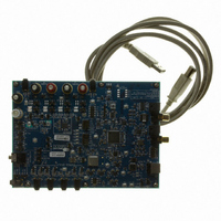
Manufacturer Part Number
CDB42L52
Description
Eval Bd LP Codec W/Class D Spkr Driver
Manufacturer
Cirrus Logic Inc
Specifications of CDB42L52
Main Purpose
Audio, CODEC
Embedded
Yes, FPGA / CPLD
Utilized Ic / Part
CS42L52
Primary Attributes
4 Stereo Audio Inputs, Stereo Line and Speaker Outputs, S/PDIF Inputs and Outputs
Secondary Attributes
GUI, I2C, SPI, USB Interfaces
Description/function
Audio CODECs
Operating Supply Voltage
5 V
Product
Audio Modules
Lead Free Status / RoHS Status
Contains lead / RoHS non-compliant
For Use With/related Products
CS42L52
Lead Free Status / RoHS Status
Contains lead / RoHS non-compliant
Other names
598-1505


DS680F1
LIST OF FIGURES
9. PCB LAYOUT CONSIDERATIONS ..................................................................................................... 77
10. ADC & DAC DIGITAL FILTERS ........................................................................................................ 78
11. PARAMETER DEFINITIONS .............................................................................................................. 79
12. PACKAGE DIMENSIONS .................................................................................................................. 80
13. ORDERING INFORMATION .............................................................................................................. 81
14. REFERENCES .................................................................................................................................... 81
15. REVISION HISTORY .......................................................................................................................... 81
Figure 1. Typical Connection Diagram ...................................................................................................... 10
Figure 2. Headphone Output Test Load .................................................................................................... 19
Figure 3. Serial Audio Interface Timing ..................................................................................................... 21
Figure 4. Control Port Timing - I²C ............................................................................................................ 22
Figure 5. Analog Input Signal Flow ........................................................................................................... 26
Figure 6. Single-Ended MIC Configuration ............................................................................................... 27
Figure 7. Differential MIC Configuration .................................................................................................... 27
Figure 8. ALC ............................................................................................................................................ 28
Figure 9. Noise Gate Attenuation .............................................................................................................. 28
Figure 10. DSP Engine Signal Flow .......................................................................................................... 29
Figure 11. PWM Output Stage .................................................................................................................. 30
Figure 12. Analog Output Stage ................................................................................................................ 30
Figure 13. Beep Configuration Options ..................................................................................................... 31
Figure 14. Peak Detect & Limiter .............................................................................................................. 32
Figure 15. Battery Compensation ............................................................................................................. 34
Figure 16. I²S Format ................................................................................................................................ 36
Figure 17. Left-Justified Format ................................................................................................................ 36
Figure 18. Right-Justified Format (DAC only) ........................................................................................... 36
Figure 19. DSP Mode Format) .................................................................................................................. 36
Figure 20. Control Port Timing, I²C Write .................................................................................................. 38
Figure 21. Control Port Timing, I²C Read .................................................................................................. 38
Figure 22. THD+N vs. Output Power per Channel at 1.8 V (16 Ω load) ................................................... 74
Figure 23. THD+N vs. Output Power per Channel at 2.5 V (16 Ω load) ................................................... 74
Figure 24. THD+N vs. Output Power per Channel at 1.8 V (32 Ω load) ................................................... 75
Figure 25. THD+N vs. Output Power per Channel at 2.5 V (32 Ω load) ................................................... 75
Figure 26. ADC Passband Ripple ............................................................................................................. 78
Figure 27. ADC Stopband Rejection ......................................................................................................... 78
Figure 28. ADC Transition Band ............................................................................................................... 78
Figure 29. ADC Transition Band (Detail) ................................................................................................... 78
Figure 30. DAC Passband Ripple ............................................................................................................. 78
Figure 31. DAC Stopband ......................................................................................................................... 78
Figure 32. DAC Transition Band ............................................................................................................... 78
Figure 33. DAC Transition Band (Detail) ................................................................................................... 78
THERMAL CHARACTERISTICS .......................................................................................................... 80
8.2 Auto Detect Disabled ...................................................................................................................... 76
9.1 Power Supply, Grounding ............................................................................................................... 77
9.2 QFN Thermal Pad .......................................................................................................................... 77
5/13/08
CS42L52
7
Related parts for CDB42L52
Image
Part Number
Description
Manufacturer
Datasheet
Request
R

Part Number:
Description:
Development Kit
Manufacturer:
Cirrus Logic Inc
Datasheet:
Part Number:
Description:
Development Kit
Manufacturer:
Cirrus Logic Inc
Datasheet:


Part Number:
Description:
High-efficiency PFC + Fluorescent Lamp Driver Reference Design
Manufacturer:
Cirrus Logic Inc
Datasheet:
Part Number:
Description:
Development Kit
Manufacturer:
Cirrus Logic Inc
Datasheet:
Part Number:
Description:
Development Kit
Manufacturer:
Cirrus Logic Inc
Datasheet:

Part Number:
Description:
Development Kit
Manufacturer:
Cirrus Logic Inc
Datasheet:
Part Number:
Description:
Development Kit
Manufacturer:
Cirrus Logic Inc
Datasheet:
Part Number:
Description:
Development Kit
Manufacturer:
Cirrus Logic Inc
Datasheet:
Part Number:
Description:
Development Kit
Manufacturer:
Cirrus Logic Inc
Datasheet:

Part Number:
Description:
EVALUATION BOARD FOR CS8427
Manufacturer:
Cirrus Logic Inc
Datasheet:

Part Number:
Description:
BOARD EVAL FOR CS8416 RCVR
Manufacturer:
Cirrus Logic Inc
Datasheet:

Part Number:
Description:
EVALUATION BOARD FOR CS8420
Manufacturer:
Cirrus Logic Inc
Datasheet:

Part Number:
Description:
KIT DEVELOPMENT EP9315 ARM9
Manufacturer:
Cirrus Logic Inc
Datasheet:

Part Number:
Description:
KIT DEVELOPMENT EP9302 ARM9
Manufacturer:
Cirrus Logic Inc
Datasheet: