CDB42L55 Cirrus Logic Inc, CDB42L55 Datasheet
CDB42L55
Specifications of CDB42L55
CDB-42L55


Related parts for CDB42L55


CDB42L55 Summary of contents
Page 1
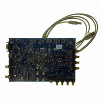
... Precision’s Programmable Serial Interface Adapter (PSIA) http://www.cirrus.com Description The CDB42L55 is the ideal evaluation platform solution to test and evaluate the CS42L55.The CS42L55 is a highly integrat- ed, 24-bit, ultra-low-power stereo CODEC based on multi-bit Delta-Sigma modulation suitable for low-power portable sys- tem applications. Use of the board requires an analog or digi- tal signal source, an analyzer, and power supplies ...
Page 2
... Analog Input Volume Tab ............................................................................................................... 13 4.4 DSP Engine Tab ............................................................................................................................. 14 4.5 Analog Output Volume Tab ............................................................................................................ 15 4.6 Register Maps Tab ......................................................................................................................... 16 5. SYSTEM CONNECTIONS AND JUMPERS ........................................................................................ 17 6. PERFORMANCE PLOTS ..................................................................................................................... 19 7. CDB42L55 BLOCK DIAGRAM ............................................................................................................ 24 8. CDB42L55 SCHEMATICS ................................................................................................................... 25 9. CDB42L55 LAYOUT ............................................................................................................................ 30 10. REVISION HISTORY .......................................................................................................................... 35 2 CDB42L55 ...
Page 3
... Figure 39.PLL, oscillator and external I/O connections (Schematic Sheet 3) ........................................... 27 Figure 40.Microcontroller and FPGA (Schematic Sheet 4) ....................................................................... 28 Figure 41.Power (Schematic Sheet 5) ...................................................................................................... 29 Figure 42.Silk Screen ................................................................................................................................ 30 Figure 43.Top-Side Layer ......................................................................................................................... 31 Figure 44.GND (Layer 2) ........................................................................................................................... 32 Figure 45.Power (Layer 3) ........................................................................................................................ 33 Figure 46.Bottom Side Layer .................................................................................................................... 34 LIST OF TABLES Table 1. System Connections ................................................................................................................... 17 Table 2. Jumper Settings .......................................................................................................................... 18 DS773DB1 CDB42L55 3 ...
Page 4
... VCP,VLDO and VA to 1.8V 5 Left pins on J109 and J104 should be shunted Monitor analog outputs via HP or Line Channel RCA Figure 1. Quick Start Board Layout CDB42L55 for details on how the various Section 4 on J48,J53,J52, J74, J7 and 3 J11 should be shunted Apply analog inputs ...
Page 5
... Power is supplied to the evaluation board through either the +5.0 V test points or the VBUS supply from the USB. NOTE: The minimum current required for board operation is approximately 300 mA. It may therefore be necessary to connect the CDB42L55 directly to the USB port on the PC as opposed to a hub or keyboard port where the current might be limited. ...
Page 6
... Section 4 “Software Mode Control” on page 10 (Figure 38 on page 26) and a discussion of the digital audio inter- software.Section 3 “Configuration Options” on page 8 provide configuration examples and software details. Section 4 on page 10 provides software configuration details. CDB42L55 and Section 4 “Software and Section 4 “Software DS773DB1 ...
Page 7
... Maps” tab of the Cirrus FlexGUI software. This tab provides low-level control of each bit. For easier configuration, additional tabs provide high-level configuration details. DS773DB1 ‘Software Mode Control” on page 10 control.‘Software Mode Control” on page 10 CDB42L55 provides con- provides 7 ...
Page 8
... CONFIGURATION OPTIONS This section highlights two common configurations for the CDB42L55. It provides a basic understanding of how the various components on the board work together. 3.1 S/PDIF or PSIA In to Analog Out The CS42L55 analog back-end performance can be tested by selecting the “SPDIF In to Analog Out -- Analog In to S/PDIF Out” ...
Page 9
... AIN1B AIN1B AIN1A AIN1A AIN2A AIN2A AIN2B AIN2B DS773DB1 FPGA PLL & Divider CS42L55 Rx SRC (CS8421) SCLK (Slave) LRCK ADC.SDOUT (Slave) Figure 3. Analog In to S/PDIF or PSIA Out CDB42L55 PSIA Rx (J40) RX.SCLK RX.LRCK RX.SDIN S/PDIF Tx (CS8406) TX.LRCK TX.SCLK S/PDIF TX.SDIN OUT (Master) 9 ...
Page 10
... Set up the signal routing in the “Board Configuration” tab as desired. 6. Set up the CS42L55 in the “CODEC...” tabs as desired. 7. Begin evaluating the CS42L55. For quick set-up, the CDB42L55 may, alternatively, be configured by loading a predefined sample script file the File menu, click "Restore Board Registers..." 9. Browse to Boards\CDB42L55\Scripts\. ...
Page 11
... Board Configuration Tab The “Board Configuration” tab provides high-level control of signal routing on the CDB42L55. The controls in this tab are used to setup the CS8416, CS8406, TxSRC, RxSRC and the FPGA Routing and are divided into separate sections or control groups for each of these individual components. A description of each con- trol group is outlined below ...
Page 12
... ADC Configuration - Controls for the input MUXs, PGA MUX’s, and high-pass filter settings. Serial Port Configuration - Controls for all settings related to the serial I/O data and clocks on the board. Update - Reads all registers in the CS42L55 and reflects the current values in the GUI. Reset - Resets the CS42L55. 12 Figure 5. CODEC Configuration Tab CDB42L55 DS773DB1 ...
Page 13
... Analog Volume Control - Analog volume controls and adjustments (PGA and MIC amps). Noise Gate Configuration - All configuration settings for the noise gate. Update - Reads all registers in the CS42L55 and reflects the current values in the GUI. Reset - Resets the CS42L55. DS773DB1 Figure 6. ADC Input Channel Volume Tab CDB42L55 13 ...
Page 14
... Tone Control - Sets the corner frequencies and the volume/gain of the treble and bass shelving filters in the DSP engine. Beep Generator - Controls for setting the various beep parameters. Update - Reads all registers in the CS42L55 and reflects the current values in the GUI. Reset - Resets the CS42L55. 14 Figure 7. DSP Engine Tab CDB42L55 DS773DB1 ...
Page 15
... Also allows one to configure the HP/Line mux to choose if the input signal to the HP/Line amplifiers comes from the DAC or the PGA. Limiter - Configuration settings for the peak detect and limiter in the codec Master Volume Control - Sets the volume of the signal out of the DSP. DS773DB1 Figure 8. Analog Output Volume Tab CDB42L55 15 ...
Page 16
... The user can change the register con- tents by using the push-buttons, by selecting a particular bit and typing in the new bit value or by selecting the register in the map and typing in a new hex value. 16 Figure 9. Register Maps Tab - CS42L55 CDB42L55 DS773DB1 ...
Page 17
... Oscillator for providing master clock for system timing Input/Output Unbuffered Digital I/O Interface to CS42L55 Intput/Output I/O bus for external I²C control port signals Table 1. System Connections CDB42L55 SIGNAL PRESENT +5V power supply GND reference GND reference Socket for +1.5 V AAA batteries Reset for microcontroller (U84) ...
Page 18
... HPOUTA * HPOUTB * Table 2. Jumper Settings CDB42L55 FUNCTION SELECTED Voltage source is +1.8 V regulator. Voltage source is +2.5 V regulator. Voltage source is +3.3 V regulator. Voltage source is +1.8V from battery. Voltage source is +1.8 V regulator. Voltage source is +2.5 V regulator. . Voltage source is +1.8V from battery. Voltage source is +1.8 V regulator. ...
Page 19
... Figure 11. THD+N vs Amplitude - Analog In to Digital Out +0 -20 - -80 S -100 -120 -140 2k 5k 10k 20k 20 Figure 13. Fig. 10 shows the THD+N vs. frequency performance measured with a CDB42L55 -50 -40 -30 -20 -10 dBr 50 100 200 500 10k Hz FFT - Analog In to Digital Out @ -60 dBFS 20k 19 ...
Page 20
... Figure 17. Fade-to-Noise Linearity - Analog In to Digital -60 -65 -70 d -75 B -80 r -85 A -90 -95 -100 2k 5k 10k 20k -100 Figure 19. CDB42L55 50 100 200 500 10k Hz FFT Crosstalk - Analog In to Digital Out @ -1 dBFS -125 -100 -75 -50 -25 dBr Out -80 -60 -40 -20 dBFS THD+N vs ...
Page 21
... A -100 -120 -140 10k 20k Figure 23. FFT - Digital Out - no input +40 +30 + -10 A -20 -30 - 10k 20k Figure 25. Fade-to-Noise Linearity- Digital Out CDB42L55 50 100 200 500 10k Hz FFT - Digital Out @ 0 dBFS 50 100 200 500 10k Hz -125 -100 -75 -50 -25 dBFS 20k 20k +0 ...
Page 22
... B r -90 A -100 -110 -20 +0 -120 -60 Figure 29. +0 -20 - -80 A -100 -120 -140 10k 20k 20 Figure 31. CDB42L55 50 100 200 500 10k Hz Master Volume (Digital) Line Volume (Analog) -50 -40 -30 -20 -10 dBr A THD+N vs. Volume - Digital In to Line Out 50 100 200 500 10k Hz FFT - Digital In to Line Out @ -60 dBFS ...
Page 23
... B r -80 A -100 -120 2k 5k 10k 20k -140 20 Figure 33. +40 +30 + -10 A -20 -30 - 10k 20k Figure 35. CDB42L55 50 100 200 500 FFT Crosstalk - Digital In to Line Out @ 0 dBFS -125 -100 -75 -50 -25 dBFS Fade-to-Noise Linearity- Digital In to Line Out 10k 20k +0 23 ...
Page 24
... CDB42L55 BLOCK DIAGRAM PC Control Board Power External 5.0 V Supply Serial USB I²C for all applicable devices Oscillator PLL FPGA S/PDIF Rx Clock/Data Routing Clock dividers and PLL used to derive all applicable Fs S/PDIF Tx from 24 MHz oscillator SRC (Tx) SRC (Rx) I/O Stake Headers for Audio Precision’ ...
Page 25
... CDB42L55 SCHEMATICS Figure 37. CS42L55 & Analog I/O (Schematic Sheet 1) ...
Page 26
Figure 38. S/PDIF & Digital Interface (Schematic Sheet 2) ...
Page 27
Figure 39. PLL, oscillator and external I/O connections (Schematic Sheet 3) ...
Page 28
Figure 40. Microcontroller and FPGA (Schematic Sheet 4) ...
Page 29
Figure 41. Power (Schematic Sheet 5) ...
Page 30
... CDB42L55 LAYOUT Figure 42. Silk Screen ...
Page 31
Figure 43. Top-Side Layer ...
Page 32
Figure 44. GND (Layer 2) ...
Page 33
Figure 45. Power (Layer 3) ...
Page 34
Figure 46. Bottom Side Layer ...
Page 35
... REVISION HISTORY Revision DB1 Initial Release DS773DB1 Changes CDB42L55 35 ...
Page 36
... Cirrus Logic, Cirrus, and the Cirrus Logic logo designs are trademarks of Cirrus Logic, Inc. All other brand and product names in this document may be trademarks or service marks of their respective owners registered trademark of Philips Semiconductor. Microsoft and Windows are registed trademarks of Microsoft Corporation. 36 www.cirrus.com. CDB42L55 DS773DB1 ...