CDB42L55 Cirrus Logic Inc, CDB42L55 Datasheet - Page 3
CDB42L55
Manufacturer Part Number
CDB42L55
Description
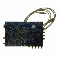
Eval Bd Ultra Low Power Stereo Codec
Manufacturer
Cirrus Logic Inc
Specifications of CDB42L55
Main Purpose
Audio, CODEC
Embedded
Yes, FPGA / CPLD
Utilized Ic / Part
CS42L55
Primary Attributes
2 Stereo Analog Inputs, Stereo Line and Headphone Outputs, S/PDIF Transmitter and Receiver
Secondary Attributes
GUI, USB, RS232, I2C Interfaces, USB or External or Battery Power Supply
Product
Audio Modules
Lead Free Status / RoHS Status
Contains lead / RoHS non-compliant
Lead Free Status / RoHS Status
Contains lead / RoHS non-compliant
Other names
598-1506
CDB-42L55
CDB-42L55


DS773DB1
LIST OF FIGURES
LIST OF TABLES
Figure 1.Quick Start Board Layout .............................................................................................................. 4
Figure 2.S/PDIF or PSIA In to Analog Out .................................................................................................. 8
Figure 3.Analog In to S/PDIF or PSIA Out .................................................................................................. 9
Figure 4.Board Configuration Tab ............................................................................................................. 11
Figure 5.CODEC Configuration Tab ......................................................................................................... 12
Figure 6.ADC Input Channel Volume Tab ................................................................................................. 13
Figure 7.DSP Engine Tab ......................................................................................................................... 14
Figure 8.Analog Output Volume Tab ......................................................................................................... 15
Figure 9.Register Maps Tab - CS42L55 ................................................................................................... 16
Figure 10.THD+N vs Freq. - Analog In to Digital Out ................................................................................ 19
Figure 11.THD+N vs Amplitude - Analog In to Digital Out ........................................................................ 19
Figure 12.FFT - Analog In to Digital Out @ -1 dBFS ................................................................................ 19
Figure 13.FFT - Analog In to Digital Out @ -60 dBFS .............................................................................. 19
Figure 14.FFT - Analog In to Digital Out - no input ................................................................................... 20
Figure 15.FFT Crosstalk - Analog In to Digital Out @ -1 dBFS ................................................................ 20
Figure 16.Freq. Response - Analog In to Digital Out ................................................................................ 20
Figure 17.Fade-to-Noise Linearity - Analog In to Digital Out .................................................................... 20
Figure 18.THD+N vs Freq. - Digital In to HP Out ...................................................................................... 20
Figure 19.THD+N vs Amplitude - Digital In to HP Out .............................................................................. 20
Figure 20.THD+N vs Volume - Digital In to HP Out .................................................................................. 21
Figure 21.FFT - Digital In to HP Out @ 0 dBFS ........................................................................................ 21
Figure 22.FFT - Digital In to HP Out @ -60 dBFS ..................................................................................... 21
Figure 23.FFT - Digital In to HP Out - no input ......................................................................................... 21
Figure 24.Freq. Response - Digital In to HP Out ...................................................................................... 21
Figure 25.Fade-to-Noise Linearity- Digital In to HP Out ............................................................................ 21
Figure 26.FFT Crosstalk - Digital In to HP Out @ 0 dBFS ........................................................................ 22
Figure 27.THD+N vs Freq. - Digital In to Line Out .................................................................................... 22
Figure 28.THD+N vs Amplitude - Digital In to Line Out ............................................................................ 22
Figure 29.THD+N vs Volume - Digital In to Line Out ................................................................................ 22
Figure 30.FFT - Digital In to Line Out @ 0 dBFS ...................................................................................... 22
Figure 31.FFT - Digital In to Line Out @ -60 dBFS ................................................................................... 22
Figure 32.FFT - Digital In to Line Out - no input ........................................................................................ 23
Figure 33.FFT Crosstalk - Digital In to Line Out @ 0 dBFS ...................................................................... 23
Figure 34.Freq. Response - Digital In to Line Out ..................................................................................... 23
Figure 35.Fade-to-Noise Linearity- Digital In to Line Out .......................................................................... 23
Figure 36.Block Diagram ........................................................................................................................... 24
Figure 37.CS42L55 & Analog I/O (Schematic Sheet 1) ............................................................................ 25
Figure 38.S/PDIF & Digital Interface (Schematic Sheet 2) ....................................................................... 26
Figure 39.PLL, oscillator and external I/O connections (Schematic Sheet 3) ........................................... 27
Figure 40.Microcontroller and FPGA (Schematic Sheet 4) ....................................................................... 28
Figure 41.Power (Schematic Sheet 5) ...................................................................................................... 29
Figure 42.Silk Screen ................................................................................................................................ 30
Figure 43.Top-Side Layer ......................................................................................................................... 31
Figure 44.GND (Layer 2) ........................................................................................................................... 32
Figure 45.Power (Layer 3) ........................................................................................................................ 33
Figure 46.Bottom Side Layer .................................................................................................................... 34
Table 1. System Connections ................................................................................................................... 17
Table 2. Jumper Settings .......................................................................................................................... 18
CDB42L55
3
Related parts for CDB42L55
Image
Part Number
Description
Manufacturer
Datasheet
Request
R

Part Number:
Description:
Development Kit
Manufacturer:
Cirrus Logic Inc
Datasheet:
Part Number:
Description:
Development Kit
Manufacturer:
Cirrus Logic Inc
Datasheet:


Part Number:
Description:
High-efficiency PFC + Fluorescent Lamp Driver Reference Design
Manufacturer:
Cirrus Logic Inc
Datasheet:
Part Number:
Description:
Development Kit
Manufacturer:
Cirrus Logic Inc
Datasheet:
Part Number:
Description:
Development Kit
Manufacturer:
Cirrus Logic Inc
Datasheet:

Part Number:
Description:
Development Kit
Manufacturer:
Cirrus Logic Inc
Datasheet:
Part Number:
Description:
Development Kit
Manufacturer:
Cirrus Logic Inc
Datasheet:
Part Number:
Description:
Development Kit
Manufacturer:
Cirrus Logic Inc
Datasheet:
Part Number:
Description:
Development Kit
Manufacturer:
Cirrus Logic Inc
Datasheet:

Part Number:
Description:
EVALUATION BOARD FOR CS8427
Manufacturer:
Cirrus Logic Inc
Datasheet:

Part Number:
Description:
BOARD EVAL FOR CS8416 RCVR
Manufacturer:
Cirrus Logic Inc
Datasheet:

Part Number:
Description:
EVALUATION BOARD FOR CS8420
Manufacturer:
Cirrus Logic Inc
Datasheet:

Part Number:
Description:
KIT DEVELOPMENT EP9315 ARM9
Manufacturer:
Cirrus Logic Inc
Datasheet:

Part Number:
Description:
KIT DEVELOPMENT EP9302 ARM9
Manufacturer:
Cirrus Logic Inc
Datasheet: