SM1211E915 Semtech, SM1211E915 Datasheet - Page 3
SM1211E915
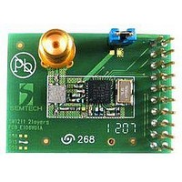
Manufacturer Part Number
SM1211E915
Description
Dev Kit Accessory
Manufacturer
Semtech
Specifications of SM1211E915
Modulation Type
FSK, OOK
Data Rate Max
200Kbps
Frequency Range
902MHz To 928MHz
Supply Voltage Range
2.1V To 3.6V
Module Interface
SPI
Supply Current
25mA
Accessory Type
RF Module
Sensitivity
-105dBm
Operating Temperature (min)
-40C
Operating Temperature (max)
85C
Operating Temperature Classification
Industrial
Package Type
TQFN EP
Operating Supply Voltage (min)
2.1V
Operating Supply Voltage (typ)
2.5/3.3V
Operating Supply Voltage (max)
3.6V
Sensitivity (dbm)
-105dBm
Rohs Compliant
NA
Lead Free Status / RoHS Status
na
Lead Free Status / RoHS Status
na


7.6.9. Pout Stability over Temperature and Voltage .................... 84
7.6.10. Transmitter Spectral Purity ............................................. 85
7.6.11. OOK Channel Bandwidth................................................ 86
7.6.12. FSK Spectrum in Europe ................................................ 87
7.6.13. Digital Modulation Schemes............................................ 88
7.6.14. Current Stability over Temperature and Voltage ............. 89
Index of Figures
Figure 1: SX1211 Simplified Block Diagram ................................. 5
Figure 2: SX1211 Pin Diagram ..................................................... 6
Figure 3: SX1211 Detailed Block Diagram.................................. 12
Figure 4: Power Supply Breakdown............................................ 13
Figure 5: Frequency Synthesizer Description.............................. 14
Figure 6: LO Generator .............................................................. 14
Figure 7: Loop Filter ................................................................... 16
Figure 8: Transmitter Architecture .............................................. 18
Figure 9: I(t), Q(t) Overview ........................................................ 18
Figure 10: PA Control ................................................................. 21
Figure 11: Optimal Load Impedance Chart ................................. 21
Figure 13: Front-end Description ................................................ 22
Figure 14: Receiver Architecture ................................................ 23
Figure 15: FSK Receiver Setting ................................................ 23
Figure 16: OOK Receiver Setting ............................................... 23
Figure 17: Active Channel Filter Description ............................... 24
Figure 18: Butterworth Filter's Actual BW ................................... 26
Figure 19: Polyphase Filter's Actual BW ..................................... 26
Figure 20: RSSI Dynamic Range................................................ 27
Figure 21: RSSI IRQ Timings ..................................................... 28
Figure 22: OOK Demodulator Description................................... 29
Figure 23: Floor Threshold Optimization ..................................... 30
Figure 24: BitSync Description.................................................... 31
Figure 25: SX1211’s Data Processing Conceptual View............. 34
Figure 26: SPI Interface Overview and uC Connections ............. 35
Figure 27: Write Register Sequence ........................................... 36
Figure 28: Read Register Sequence........................................... 37
Figure 29: Write Bytes Sequence (ex: 2 bytes) ........................... 37
Figure 30: Read Bytes Sequence (ex: 2 bytes)........................... 38
Figure 31: FIFO and Shift Register (SR) ..................................... 38
Figure 32: FIFO Threshold IRQ Source Behavior ....................... 39
Figure 33: Sync Word Recognition ............................................. 40
Figure 34: Continuous Mode Conceptual View ........................... 41
Figure 35: Tx Processing in Continuous Mode............................ 41
Figure 36: Rx Processing in Continuous Mode ........................... 42
Figure 37: uC Connections in Continuous Mode......................... 43
Figure 38: Buffered Mode Conceptual View................................ 44
Figure 39: Tx processing in Buffered Mode ................................ 45
Figure 40: Rx Processing in Buffered Mode................................ 46
Figure 41: uC Connections in Buffered Mode ............................. 47
Figure 42: Packet Mode Conceptual View .................................. 49
Figure 43: Fixed Length Packet Format...................................... 50
Figure 44: Variable Length Packet Format.................................. 51
Figure 45: CRC Implementation ................................................. 53
Rev 7 – Sept 2
Figure 12: Recommended PA Biasing and Output Matching ..... 22
ADVANCED COMMUNICATIONS & SENSING
nd
, 2008
Page 3 of 92
8. Packaging Information ............................................................ 90
8.1. Package Outline Drawing..................................................... 90
8.2. PCB Land Pattern................................................................ 90
8.3. Tape & Reel Specification.................................................... 91
9. Revision History...................................................................... 92
10. Contact Information .............................................................. 92
Figure 46: Manchester Encoding/Decoding ................................ 54
Figure 47: Data Whitening .......................................................... 54
Figure 48: uC Connections in Packet Mode ................................ 55
Figure 49: Optimized Rx Cycle ................................................... 67
Figure 50: Optimized Tx Cycle.................................................... 68
Figure 51: Tx Hop Cycle ............................................................. 69
Figure 52: Rx Hop Cycle............................................................. 70
Figure 53: Rx
Figure 54: POR Timing Diagram................................................. 72
Figure 55: Manual Reset Timing Diagram................................... 72
Figure 56: Reference Design Circuit Schematic.......................... 73
Figure 57: Reference Design‘s Stackup...................................... 74
Figure 58: Reference Design Layout (top view) .......................... 74
Figure 59: 915 MHz SAW Filter Plot ........................................... 75
Figure 60: 869 MHz SAW Filter Plot ........................................... 75
Figure 61: Sensitivity Across the 868 MHz Band......................... 77
Figure 62: Sensitivity Across the 915 MHz Band......................... 77
Figure 63: FSK Sensitivity Loss vs. LO Drift................................ 78
Figure 64: OOK Sensitivity Loss vs. LO Drift............................... 78
Figure 65: FSK Sensitivity vs. Rx BW ......................................... 79
Figure 66: OOK Sensitivity Change vs. Rx BW ........................... 79
Figure 67: Sensitivity Stability ..................................................... 80
Figure 68: FSK Sensitivity vs. BR ............................................... 80
Figure 69: OOK Sensitivity vs. BR .............................................. 81
Figure 70: ACR in FSK Mode...................................................... 81
Figure 71: ACR in OOK Mode..................................................... 82
Figure 72: Pout for 869 MHz Band Operation ............................. 82
Figure 73: Pout for 915 MHz Band Operation ............................. 83
Figure 74: Pout and IDD at all PA Settings, 869 MHz ................. 83
Figure 75: Pout and IDD at all PA Settings, 915 MHz ................. 84
Figure 76: Pout Stability.............................................................. 84
Figure 77: 869 MHz Spectral Purity DC-1GHz ............................ 85
Figure 78: 869 MHz Spectral Purity 1-6GHz ............................... 85
Figure 79: OOK Spectrum - 2kbps.............................................. 86
Figure 80: OOK Spectrum - 8kbps.............................................. 86
Figure 81: OOK Spectrum - 16.7kbps ......................................... 86
Figure 82: FSK - 1.56kbps - +/-33 kHz........................................ 87
Figure 83: FSK - 25 kbps - +/-50 kHz.......................................... 87
Figure 84: FSK - 40 kbps - +/-40 kHz.......................................... 87
Figure 85: DTS 6dB Bandwidth................................................... 88
Figure 86: DTS Power Spectral Density...................................... 88
Figure 87: IDD vs. Temp and VDD.............................................. 89
Figure 88: Package Outline Drawing........................................... 90
Figure 89: PCB Land Pattern...................................................... 90
Figure 90: Tape & Reel Dimensions ........................................... 91
Tx
Rx Cycle ................................................. 71
www.semtech.com
SX1211
Related parts for SM1211E915
Image
Part Number
Description
Manufacturer
Datasheet
Request
R

Part Number:
Description:
Ultra Low Power Integrated Uhf Transceiver Module
Manufacturer:
Semtech Corporation
Datasheet:


Part Number:
Description:
TVS 300W 12V SOT-23
Manufacturer:
Micro Commercial Components (MCC)
Datasheet:

Part Number:
Description:
EVALUATION BOARD
Manufacturer:
Semtech
Datasheet:
Part Number:
Description:
EVALUATION BOARD
Manufacturer:
Semtech
Datasheet:
Part Number:
Description:
VOLTAGE SUPPRESSOR, TRANSIENT SEMTECH
Manufacturer:
Semtech
Datasheet:
Part Number:
Description:
HIGH VOLTAGE CAPACITORS MONOLITHIC CERAMIC TYPE
Manufacturer:
Semtech Corporation
Datasheet:
Part Number:
Description:
EZ1084CM5.0 AMP POSITIVE VOLTAGE REGULATOR
Manufacturer:
Semtech Corporation
Datasheet:
Part Number:
Description:
3.0 AMP LOW DROPOUT POSITIVE VOLTAGE REGULATORS
Manufacturer:
Semtech Corporation
Datasheet:
Part Number:
Description:
Manufacturer:
Semtech Corporation
Datasheet:
Part Number:
Description:
RailClamp Low Capacitance TVS Diode Array
Manufacturer:
Semtech Corporation
Datasheet:
Part Number:
Description:
Manufacturer:
Semtech Corporation
Datasheet:
Part Number:
Description:
Manufacturer:
Semtech Corporation
Datasheet: