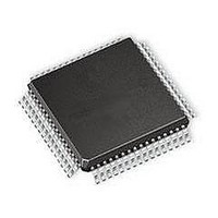
NJU6535FH1 NJR, NJU6535FH1 Datasheet - Page 12

NJU6535FH1
Manufacturer Part Number
NJU6535FH1
Description
LCD Drivers 1/3 1/4 LCD
Manufacturer
NJR
Datasheet
1.NJU6535FH1.pdf
(30 pages)
Specifications of NJU6535FH1
Operating Supply Voltage
5.5 V
Maximum Operating Temperature
+ 70 C
Package / Case
PQFP-H1
Minimum Operating Temperature
0 C
Lead Free Status / RoHS Status
Lead free / RoHS Compliant
Available stocks
Company
Part Number
Manufacturer
Quantity
Price
Company:
Part Number:
NJU6535FH1
Manufacturer:
JRC
Quantity:
8 861
NJU6535
(5) Power save mode
(6)
(6-3)
- 12 -
In power save mode, segment drivers and commons output “L” level and the internal oscillation circuit is stop
the operation ( but operates at Key in detection) for operation current reduction.
P1 in power save mode. (refer (1)Instruction (e)Segment output / General output port)
the number of keys in key-matrix by “Segment output / key scan output select” instruction.
It outputs a identified key data to CPU after comparison with two data read from the key-matrix in twice for
reliable key operation. If those data are not identified, key data is not outputted. It outputs “L” signal through
“SO” terminal as the request after 577T[s] (T=1/fosc) when any key is operated. Furthermore, the key scan
circuit structures for reducing the external components like as Diodes to prevent circuit short problem.
case of 25 keys application, unassigned area from KD1 to KD5 take “0” signal also.
save 2, area from KD1 to KD20 take “0” signal also. The terminals, which are not connected any keys, should be
signal of CE terminal.
Power save in Key data reading and sets “0” in mode of Normal.
(6-1) The relation between output data and key matrix
(6-2) Data output timing
Power save mode 1 to 3 is set by “1” level as a control data in PS0 or 1, and released by “0” in PS0 and PS1.
However, output terminals SEG1/P0 to SEG4/P3 operate as General output port set by control data P0 and
The status of Power save flag is outputted after KD30 in Key data reading. This flag sets “1” signal in mode of
Key scan circuit connects the 6 x 5 key-matrix maximum and reads the data of 30 keys maximum. It chooses
The relation between output data and key matrix shows bellow table and sets “1” signal for operated key.
In case of 20 keys application, unassigned area for keys from KD1 to KD10 in bellow table take “0” signal. In
In mode of Power save 1, area for keys from KD1 to KD25 in bellow table take “0” signal. In mode of Power
The data output format shows bellow. The data output mode is set by “L” status of SCL terminal at the rising
Key scan circuit
CE
SCL
SI
SO
Power save flag(PSF)
S0
S1
S2
S3
S4
S5
KD11
KD16
KD21
KD26
KD1
KD6
K0
* KD1 KD2
KD12
KD17
KD22
KD27
KD2
KD7
K1
KD13
KD18
KD23
KD28
KD3
KD8
K2
Key data
KD14
KD19
KD24
KD29
KD4
KD9
K3
KD10
KD15
KD20
KD25
KD30
KD5
K4
KD29 KD30 PSF
Ver.2004-04-16
open.


