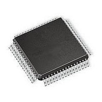
NJU6535FH1 NJR, NJU6535FH1 Datasheet - Page 3

NJU6535FH1
Manufacturer Part Number
NJU6535FH1
Description
LCD Drivers 1/3 1/4 LCD
Manufacturer
NJR
Datasheet
1.NJU6535FH1.pdf
(30 pages)
Specifications of NJU6535FH1
Operating Supply Voltage
5.5 V
Maximum Operating Temperature
+ 70 C
Package / Case
PQFP-H1
Minimum Operating Temperature
0 C
Lead Free Status / RoHS Status
Lead free / RoHS Compliant
Available stocks
Company
Part Number
Manufacturer
Quantity
Price
Company:
Part Number:
NJU6535FH1
Manufacturer:
JRC
Quantity:
8 861
!
Ver.2004-04-16
TERMINAL DESCRIPTION 1
50 to 54
5 to 39
No.
40
41
42
43
44
45
46
47
48
49
55
56
57
58
59
60
61
62
63
64
1
2
3
4
SEG5 to
SEG40/COM4
SEG41/S0
SEG42/S1
SYMBOL
SEG1/P0
SEG2/P1
SEG3/P2
SEG4/P3
S2 to S6
K0 to K4
COM1
COM2
COM3
OSC
SCL
V
V
SO
CE
V
V
V
SEG39
SI
DD
SS
0
1
2
I/O
I/O
O
O
O
O
O
O
O
-
-
I
I
I
I
I
LCD Segment output terminal / General output terminal.
Select Segment output terminal or General output terminal by the instruction.
LCD Segment output terminal
LCD Common output terminal
LCD Segment output terminal / LCD Common output terminal
SEG40 in 1/3Duty use, COM4 in 1/4Duty use.
LCD Segment output terminals / key scanning output terminals
Select Segment output terminal or key scanning output terminal by the
instruction. (No need for anti-reverse current diode in key scan)
Key scanning output terminals.
Key scanning input terminals.
Power source: VDD=5V with LCD driving voltage input.
LCD driving voltage stabilization capacitor terminals.
In use of 1/2 bias, connects V
GND: VSS=0V
System clock input terminal
This terminal should be open for internal clock operation.
Change Oscillation frequency by connecting capacitor and resistor. Inputs
external oscillation clock.
Data output terminal.
Chip enable terminal.
Shift clock input terminal.
Data input terminal.
(No need for anti-reverse current diode in key scan)
(with internal pull-down resistor)
1
to V
FUNCTION
2.
NJU6535
- 3 -


