MA160014 Microchip Technology, MA160014 Datasheet - Page 100
MA160014
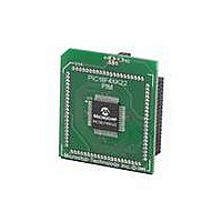
Manufacturer Part Number
MA160014
Description
MOD PLUG-IN 44PIN PIC18LF45K22
Manufacturer
Microchip Technology
Series
PIC® XLP™ 18Fr
Datasheet
1.PIC18F26J13-ISS.pdf
(496 pages)
Specifications of MA160014
Accessory Type
Plug-In Module (PIM) - PIC18LF45K10
Product
Microcontroller Modules
Data Bus Width
8 bit
Core Processor
PIC18LF45K22
Interface Type
I2C, SPI
Operating Supply Voltage
1.8 V to 5.5 V
Lead Free Status / RoHS Status
Lead free / RoHS Compliant
For Use With/related Products
PICDEM PIC18 Explorer, DM183032
Lead Free Status / Rohs Status
Lead free / RoHS Compliant
Available stocks
Company
Part Number
Manufacturer
Quantity
Price
Company:

Part Number:
MA160014
Manufacturer:
Microchip Technology
Quantity:
135
Company:
Part Number:
MA160014
Manufacturer:
MICROCHIP
Quantity:
12 000


PIC18(L)F2X/4XK22
6.4
The minimum erase block is 32 words or 64 bytes. Only
through the use of an external programmer, or through
ICSP™ control, can larger blocks of program memory
be bulk erased. Word erase in the Flash array is not
supported.
When
microcontroller itself, a block of 64 bytes of program
memory is erased. The Most Significant 16 bits of the
TBLPTR<21:6> point to the block being erased. The
TBLPTR<5:0> bits are ignored.
The EECON1 register commands the erase operation.
The EEPGD bit must be set to point to the Flash
program memory. The WREN bit must be set to enable
write operations. The FREE bit is set to select an erase
operation.
The write initiate sequence for EECON2, shown as
steps 4 through 6 in
Memory Erase
accidental writes. This is sometimes referred to as a
long write.
A long write is necessary for erasing the internal Flash.
Instruction execution is halted during the long write
cycle. The long write is terminated by the internal
programming timer.
EXAMPLE 6-2:
DS41412D-page 100
Required
Sequence
initiating
Erasing Flash Program Memory
ERASE_BLOCK
Sequence”, is used to guard against
an
Section 6.4.1 “Flash Program
ERASING A FLASH PROGRAM MEMORY BLOCK
MOVLW
MOVWF
MOVLW
MOVWF
MOVLW
MOVWF
BSF
BCF
BSF
BSF
BCF
MOVLW
MOVWF
MOVLW
MOVWF
BSF
BSF
erase
sequence
CODE_ADDR_UPPER
TBLPTRU
CODE_ADDR_HIGH
TBLPTRH
CODE_ADDR_LOW
TBLPTRL
EECON1, EEPGD
EECON1, CFGS
EECON1, WREN
EECON1, FREE
INTCON, GIE
55h
EECON2
0AAh
EECON2
EECON1, WR
INTCON, GIE
from
Preliminary
the
6.4.1
The sequence of events for erasing a block of internal
program memory is:
1.
2.
3.
4.
5.
6.
7.
8.
; load TBLPTR with the base
; address of the memory block
; point to Flash program memory
; access Flash program memory
; enable write to memory
; enable block Erase operation
; disable interrupts
; write 55h
; write 0AAh
; start erase (CPU stall)
; re-enable interrupts
Load Table Pointer register with address of
block being erased.
Set the EECON1 register for the erase operation:
• set EEPGD bit to point to program memory;
• clear the CFGS bit to access program memory;
• set WREN bit to enable writes;
• set FREE bit to enable the erase.
Disable interrupts.
Write 55h to EECON2.
Write 0AAh to EECON2.
Set the WR bit. This will begin the block erase
cycle.
The CPU will stall for duration of the erase
(about 2 ms using internal timer).
Re-enable interrupts.
FLASH PROGRAM MEMORY
ERASE SEQUENCE
2010 Microchip Technology Inc.
Related parts for MA160014
Image
Part Number
Description
Manufacturer
Datasheet
Request
R

Part Number:
Description:
Manufacturer:
Microchip Technology Inc.
Datasheet:
Part Number:
Description:
Manufacturer:
Microchip Technology Inc.
Datasheet:
Part Number:
Description:
Manufacturer:
Microchip Technology Inc.
Datasheet:
Part Number:
Description:
Manufacturer:
Microchip Technology Inc.
Datasheet:
Part Number:
Description:
Manufacturer:
Microchip Technology Inc.
Datasheet:
Part Number:
Description:
Manufacturer:
Microchip Technology Inc.
Datasheet:
Part Number:
Description:
Manufacturer:
Microchip Technology Inc.
Datasheet:
Part Number:
Description:
Manufacturer:
Microchip Technology Inc.
Datasheet: