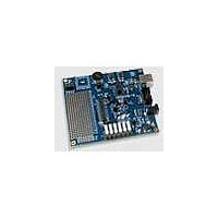
C8051F206DK-G Silicon Laboratories Inc, C8051F206DK-G Datasheet - Page 36

C8051F206DK-G
Manufacturer Part Number
C8051F206DK-G
Description
MCU, MPU & DSP Development Tools MCU DEVELOPMENT KIT W/ GLOBAL POWER SPLY
Manufacturer
Silicon Laboratories Inc
Datasheet
1.C8051F226DK.pdf
(146 pages)
Specifications of C8051F206DK-G
Processor To Be Evaluated
C8051F206
Data Bus Width
8 bit
Interface Type
USB
Lead Free Status / RoHS Status
Lead free / RoHS Compliant
- Current page: 36 of 146
- Download datasheet (2Mb)
C8051F2xx
36
Bit7:
Bit6:
Bit5:
Bit4:
Bits3–2: ADSTM1–0: ADC Start of Conversion Mode Bits
Bit1:
Bit0:
ADCEN
R/W
Bit7
SFR Definition 5.3. ADC0CN: ADC Control (C8051F220/1/6 and C8051F206)
ADCEN: ADC Enable Bit
0: ADC Disabled. ADC is in low power shutdown.
1: ADC Enabled. ADC is active and ready for data conversions.
ADCTM: ADC Track Mode Bit
0: When the ADC is enabled, tracking is continuous unless a conversion is in process
1: Tracking Defined by ADSTM1-0 bits
ADCINT: ADC Conversion Complete Interrupt Flag (cleared by software).
0: ADC has not completed a data conversion since the last time this flag was cleared
1: ADC has completed a data conversion
ADBUSY: ADC Busy Bit
Read
0: ADC Conversion complete or no valid data has been converted since a reset. The falling
edge of ADBUSY generates an interrupt when enabled.
1: ADC Busy converting data
Write
0: No effect
1: Starts ADC Conversion if ADSTM1-0 = 00b
00: ADC conversion started upon a write of 1 to ADBUSY
01: RESERVED
10: RESERVED
11: ADC conversions initiated on overflows of Timer 2
ADWINT: ADC Window Compare Interrupt Flag
0: ADC Window Comparison Data match has not occurred
1: ADC Window Comparison Data match occurred
ADLJST: ADC Left Justify Data Bit (Used on C8051F206 only)
0: Data in ADC0H:ADC0L registers are right justified.
1: Data in ADC0H:ADC0L registers are left justified.
ADCTM
R/W
Bit6
ADSTM1-0:
00: Tracking starts with the write of 1 to ADBUSY and lasts for 3 SAR clocks
01: RESERVED
10: RESERVED
11: Tracking started by the overflow of Timer 2 and last for 3 SAR clocks
ADCINT ADBUSY ADSTM1 ADSTM0 ADWINT
R/W
Bit5
R/W
Bit4
R/W
Bit3
Rev. 1.6
R/W
Bit2
R/W
Bit1
(bit addressable)
ADLJST
R/W
Bit0
SFR Address:
Reset Value
00000000
0xE8
Related parts for C8051F206DK-G
Image
Part Number
Description
Manufacturer
Datasheet
Request
R
Part Number:
Description:
SMD/C°/SINGLE-ENDED OUTPUT SILICON OSCILLATOR
Manufacturer:
Silicon Laboratories Inc
Part Number:
Description:
Manufacturer:
Silicon Laboratories Inc
Datasheet:
Part Number:
Description:
N/A N/A/SI4010 AES KEYFOB DEMO WITH LCD RX
Manufacturer:
Silicon Laboratories Inc
Datasheet:
Part Number:
Description:
N/A N/A/SI4010 SIMPLIFIED KEY FOB DEMO WITH LED RX
Manufacturer:
Silicon Laboratories Inc
Datasheet:
Part Number:
Description:
N/A/-40 TO 85 OC/EZLINK MODULE; F930/4432 HIGH BAND (REV E/B1)
Manufacturer:
Silicon Laboratories Inc
Part Number:
Description:
EZLink Module; F930/4432 Low Band (rev e/B1)
Manufacturer:
Silicon Laboratories Inc
Part Number:
Description:
I°/4460 10 DBM RADIO TEST CARD 434 MHZ
Manufacturer:
Silicon Laboratories Inc
Part Number:
Description:
I°/4461 14 DBM RADIO TEST CARD 868 MHZ
Manufacturer:
Silicon Laboratories Inc
Part Number:
Description:
I°/4463 20 DBM RFSWITCH RADIO TEST CARD 460 MHZ
Manufacturer:
Silicon Laboratories Inc
Part Number:
Description:
I°/4463 20 DBM RADIO TEST CARD 868 MHZ
Manufacturer:
Silicon Laboratories Inc
Part Number:
Description:
I°/4463 27 DBM RADIO TEST CARD 868 MHZ
Manufacturer:
Silicon Laboratories Inc
Part Number:
Description:
I°/4463 SKYWORKS 30 DBM RADIO TEST CARD 915 MHZ
Manufacturer:
Silicon Laboratories Inc
Part Number:
Description:
N/A N/A/-40 TO 85 OC/4463 RFMD 30 DBM RADIO TEST CARD 915 MHZ
Manufacturer:
Silicon Laboratories Inc
Part Number:
Description:
I°/4463 20 DBM RADIO TEST CARD 169 MHZ
Manufacturer:
Silicon Laboratories Inc


