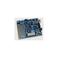
C8051F206DK-G Silicon Laboratories Inc, C8051F206DK-G Datasheet - Page 50

C8051F206DK-G
Manufacturer Part Number
C8051F206DK-G
Description
MCU, MPU & DSP Development Tools MCU DEVELOPMENT KIT W/ GLOBAL POWER SPLY
Manufacturer
Silicon Laboratories Inc
Datasheet
1.C8051F226DK.pdf
(146 pages)
Specifications of C8051F206DK-G
Processor To Be Evaluated
C8051F206
Data Bus Width
8 bit
Interface Type
USB
Lead Free Status / RoHS Status
Lead free / RoHS Compliant
- Current page: 50 of 146
- Download datasheet (2Mb)
C8051F2xx
7.
The voltage reference circuit selects between an externally connected reference and the power supply
voltage (V
An external reference can be connected to the VREF pin and selected by setting the REF0CN special
function register per Figure 7.1. The external reference supply must be between V
may also be selected using REF0CN per SFR Definition 7.1. The electrical specifications for the Voltage
Reference are given in Table 7.1.
50
Bits7–2: UNUSED. Read = 00000b; Write = don't care
Bit1–0:
R/W
Bit7
Voltage Reference (C8051F206/220/221/226)
-
Vref (external)
DD
REFSL1– REFSL0: Voltage reference selection.
Bits control which reference is selected.
00: External VREF source is selected.
01: Reserved.
10: Reserved.
11: V
). (See Figure 7.1).
Vdd
R/W
Bit6
Figure 7.1. Voltage Reference Functional Block Diagram
DD
-
selected as VREF source.
SFR Definition 7.1. REF0CN: Reference Control
R/W
Bit5
-
R/W
Bit4
-
Rev. 1.6
R/W
Bit3
-
2
R/W
Bit2
-
REFSL1
Set REF0CN to:
00: Use external Vref
11: Use Vdd
REF0CN[1:0]
R/W
Bit1
DD
REFSL0
R/W
Bit0
– 0.3 V and 1 V. V
To ADC Ref
SFR Address:
Reset Value
00000000
0xD1
DD
Related parts for C8051F206DK-G
Image
Part Number
Description
Manufacturer
Datasheet
Request
R
Part Number:
Description:
SMD/C°/SINGLE-ENDED OUTPUT SILICON OSCILLATOR
Manufacturer:
Silicon Laboratories Inc
Part Number:
Description:
Manufacturer:
Silicon Laboratories Inc
Datasheet:
Part Number:
Description:
N/A N/A/SI4010 AES KEYFOB DEMO WITH LCD RX
Manufacturer:
Silicon Laboratories Inc
Datasheet:
Part Number:
Description:
N/A N/A/SI4010 SIMPLIFIED KEY FOB DEMO WITH LED RX
Manufacturer:
Silicon Laboratories Inc
Datasheet:
Part Number:
Description:
N/A/-40 TO 85 OC/EZLINK MODULE; F930/4432 HIGH BAND (REV E/B1)
Manufacturer:
Silicon Laboratories Inc
Part Number:
Description:
EZLink Module; F930/4432 Low Band (rev e/B1)
Manufacturer:
Silicon Laboratories Inc
Part Number:
Description:
I°/4460 10 DBM RADIO TEST CARD 434 MHZ
Manufacturer:
Silicon Laboratories Inc
Part Number:
Description:
I°/4461 14 DBM RADIO TEST CARD 868 MHZ
Manufacturer:
Silicon Laboratories Inc
Part Number:
Description:
I°/4463 20 DBM RFSWITCH RADIO TEST CARD 460 MHZ
Manufacturer:
Silicon Laboratories Inc
Part Number:
Description:
I°/4463 20 DBM RADIO TEST CARD 868 MHZ
Manufacturer:
Silicon Laboratories Inc
Part Number:
Description:
I°/4463 27 DBM RADIO TEST CARD 868 MHZ
Manufacturer:
Silicon Laboratories Inc
Part Number:
Description:
I°/4463 SKYWORKS 30 DBM RADIO TEST CARD 915 MHZ
Manufacturer:
Silicon Laboratories Inc
Part Number:
Description:
N/A N/A/-40 TO 85 OC/4463 RFMD 30 DBM RADIO TEST CARD 915 MHZ
Manufacturer:
Silicon Laboratories Inc
Part Number:
Description:
I°/4463 20 DBM RADIO TEST CARD 169 MHZ
Manufacturer:
Silicon Laboratories Inc


