PC404A-2014 TAOS, PC404A-2014 Datasheet - Page 2
PC404A-2014
Manufacturer Part Number
PC404A-2014
Description
Optical Sensor Development Tools Evaluation Module TSL2014
Manufacturer
TAOS
Datasheet
1.PC404A-1401R.pdf
(3 pages)
Specifications of PC404A-2014
Operating Voltage
5 V
Description/function
Linear Sensor Array
For Use With/related Products
TSL2014
Lead Free Status / RoHS Status
Lead free / RoHS Compliant


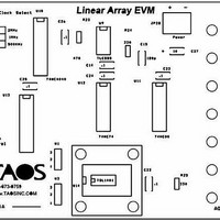
be selected from 2 MHz, 1 MHz and 500 kHz by moving the clock select jumper to the desired
position (see Figure 1). U10, U11, and U12 generate the serial input (SI) pulse with the proper
relationship to the clock (see Figure 2). The sensor integration time, defined by the time
between SI clock pulses, may be selected from 128uS to 64mS by placing the jumper at the
appropriate location.
The analog output (AO) pin of the linear array is routed to the AO test terminal on the right side
of the board, as are SI, clock (CLK), and serial out (SO) signals. The SO signal is generated by
the linear array device (applies to TSL202, TSL208, TSL1402, TSL1406, and TSL1410 only).
A supply terminal (DVdd) and 2 GND terminals are provided for applying +5 volts and
common ground. Power may be applied through terminal block JP28 if desired.
The analog output voltage is directly proportional to the light intensity and the integration time
up to the devices saturation level (3.5V typ). The proportionality constant is the responsivity of
2
the device given in (V*cm
/uW*sec). Responsivity is wavelength dependent. For the linear
arrays the responsivity will peak at about 770nm.
0
1
2
128
129
CLK
SI
1
2
128
AO
Figure 2 - System Timing (AO output for TSL1401 shown)
3. Operation
To operate the PC404A, apply 5VDC to the board using a regulated lab power supply. Connect
an oscilloscope probe to the Ao terminal and the scope ground to one of the GND terminals.
For best results, connect another probe to the SI terminal and use that signal to trigger the
oscilloscope.
Related parts for PC404A-2014
Image
Part Number
Description
Manufacturer
Datasheet
Request
R

Part Number:
Description:
Optical Sensor Development Tools Evaluation Module TSL1401
Manufacturer:
TAOS
Datasheet:
Part Number:
Description:
Optical Sensor Development Tools Evaluation Module TSL1402
Manufacturer:
TAOS
Datasheet:
Part Number:
Description:
Optical Sensor Development Tools Evaluation Module TSL202
Manufacturer:
TAOS
Datasheet:
Part Number:
Description:
Optical Sensor Development Tools Evaluation Module TSL201
Manufacturer:
TAOS
Datasheet:
Part Number:
Description:
Optical Sensor Development Tools Evaluation Module TSL208
Manufacturer:
TAOS
Datasheet:
Part Number:
Description:
Optical Sensor Development Tools TSL202 Evaluation Module
Manufacturer:
TAOS
Datasheet:
Part Number:
Description:
Optical Sensor Development Tools Evaluation Module TSL1406
Manufacturer:
TAOS
Datasheet:
Part Number:
Description:
Optical Sensor Development Tools Evaluation Module TSL210R
Manufacturer:
TAOS
Datasheet:
Part Number:
Description:
Optical Sensor Development Tools Evaluation Module TSL1410
Manufacturer:
TAOS
Datasheet:

Part Number:
Description:
Power Transformer
Manufacturer:
Superworld Electronics
Datasheet:
Part Number:
Description:
Power Transformer
Manufacturer:
Superworld Electronics
Datasheet:
Part Number:
Description:
Power Transformer
Manufacturer:
Superworld Electronics
Datasheet:
Part Number:
Description:
Power Transformer
Manufacturer:
Superworld Electronics
Datasheet:
Part Number:
Description:
Power Transformer
Manufacturer:
Superworld Electronics
Datasheet:

Part Number:
Description:
Industrial Optical Sensors Ambient Light Sensor SMBus
Manufacturer:
TAOS
Datasheet: