AD565AKD Analog Devices Inc, AD565AKD Datasheet
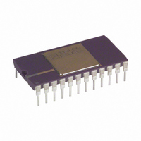
D/A Converter (D-A) IC

AD565AKD

Manufacturer Part Number
AD565AKD
Description
D/A Converter (D-A) IC
Manufacturer
Analog Devices Inc
Datasheet

Specifications of AD565AKD

No. Of Bits
12 Bit
Mounting Type
Through Hole
Interface Type
Serial
Package / Case
24-CDIP
Rohs Status
RoHS non-compliant
Settling Time
250ns
Number Of Bits
12
Data Interface
Parallel
Number Of Converters
1
Voltage Supply Source
Single Supply
Power Dissipation (max)
345mW
Operating Temperature
0°C ~ 70°C
Lead Free Status / RoHS Status

Available stocks

Company
Part Number
Manufacturer
Quantity
Price
Part Number:
AD565AKD
Manufacturer:
XILINX
Quantity:
15
Part Number:
AD565AKD
Manufacturer:
ADI
Quantity:
835
a
PRODUCT DESCRIPTION
The AD565A and AD566A are fast 12-bit digital-to-analog
converters that incorporate the latest advances in analog circuit
design to achieve high speeds at low cost.
The AD565A and AD566A use 12 precision, high speed bipolar
current-steering switches, a control amplifier, and a laser-trimmed
thin-film resistor network to produce a very fast, high accuracy
analog output current. The AD565A also includes a buried
Zener reference that features low noise, long-term stability, and
temperature drift characteristics comparable to the best discrete
reference diodes.
The combination of performance and flexibility in the AD565A and
AD566A has resulted from major innovations in circuit design,
an important new high speed bipolar process, and continuing
advances in laser-wafer-trimming techniques (LWT). The
AD565A and AD566A have a 10%–90% full-scale transition
time less than 35 ns and settle to within ±1/2 LSB in 250 ns max
(350 ns for AD566A). Both are laser-trimmed at the wafer level
to ± 1/8 LSB typical linearity and are specified to ± 1/4 LSB max
error (K and T grades) at +25°C. High speed and accuracy make
the AD565A and AD566A the ideal choice for high speed display
drivers as well as for fast analog-to-digital converters.
The laser trimming process that provides the excellent linearity
is also used to trim both the absolute value and the temperature
coefficient of the reference of the AD565A, resulting in a typical
full-scale gain TC of 10 ppm/°C. When tighter TC performance
is required or when a system reference is available, the AD566A
may be used with an external reference.
REV. E
Information furnished by Analog Devices is believed to be accurate and
reliable. However, no responsibility is assumed by Analog Devices for its
use, nor for any infringements of patents or other rights of third parties that
may result from its use. No license is granted by implication or otherwise
under any patent or patent rights of Analog Devices.
FEATURES
Single Chip Construction
Very High Speed Settling to 1/2 LSB
Full-Scale Switching Time: 30 ns
Guaranteed for Operation with
Linearity Guaranteed Overtemperature
Monotonicity Guaranteed Overtemperature
Low Power: AD566A = 180 mW max;
Use with On-Board High Stability Reference (AD565A)
Low Cost
MlL-STD-883-Compliant Versions Available
AD565A: 250 ns max
AD566A: 350 ns max
1/2 LSB max (K, T Grades)
with –12 V Supply (AD566A)
or with External Reference (AD566A)
AD565A = 225 mW max
12 V (565A) Supplies,
AD565A and AD566A are available in four performance
grades. The J and K grades are specified for use over the 0°C to
+70°C temperature range while the S and T grades are speci-
fied for the –55°C to +125°C range. The D grades are all pack-
aged in a 24-lead, hermetically sealed, ceramic, dual-in-line
package. The JR grade is packaged in a 28-lead plastic SOIC.
PRODUCT HIGHLIGHTS
1. The wide output compliance range of the AD565A and
2. The devices incorporate a newly developed, fully differential,
3. The devices also contain SiCr thin-film application resistors
4. The AD565A and AD566A are available in versions compliant
One Technology Way, P.O. Box 9106, Norwood, MA 02062-9106, U.S.A.
Tel:
Fax: 781/326-8703
GND
GND
REF
REF
REF
REF
IN
IN
AD566A are ideally suited for fast, low noise, accurate voltage
output configurations without an output amplifier.
nonsaturating precision current switching cell structure that
combines the dc accuracy and stability first developed in the
AD562/AD563 with very fast switching times and an optimally
damped settling characteristic.
that can be used with an external op amp to provide a preci-
sion voltage output or as input resistors for a successive-
approximation A/D converter. The resistors are matched to
the internal ladder network to guarantee a low gain temperature
coefficient and are laser-trimmed for minimum full-scale and
bipolar offset errors.
with MIL-STD-883. Refer to the Analog Devices Military
Products Databook or current /883B data sheet for detailed
specifications.
781/329-4700
REF OUT
19.95k
20k
19.95k
20k
Monolithic D/A Converters
–V
–V
10V
FUNCTIONAL BLOCK DIAGRAMS
EE
EE
V
CC
POWER
POWER
GND
GND
0.5mA
0.5mA
I
I
REF
REF
AD565A/AD566A
AD566A
AD565A
MSB
MSB
High Speed 12-Bit
CODE INPUT
CODE INPUT
I
4
I
4
OUT
OUT
I
I
REF
REF
=
=
DAC
DAC
© Analog Devices, Inc., 2002
CODE
CODE
9.95k
9.95k
LSB
LSB
BIPOLAR OFF
BIPOLAR OFF
I
I
O
O
www.analog.com
5k
5k
5k
5k
8k
8k
20V SPAN
10V SPAN
DAC OUT
20V SPAN
10V SPAN
DAC OUT

Related parts for AD565AKD

AD565AKD Summary of contents

Page 1

FEATURES Single Chip Construction Very High Speed Settling to 1/2 LSB AD565A: 250 ns max AD566A: 350 ns max Full-Scale Switching Time Guaranteed for Operation with with –12 V Supply (AD566A) Linearity Guaranteed Overtemperature 1/2 LSB max ...

Page 2

AD565A–SPECIFICATIONS Parameter 1 DATA INPUTS (Pins 13 to 24) TTL CMOS Input Voltage Bit ON Logic “1” Bit OFF Logic “0” Logic Current (Each Bit) Bit ON Logic “1” Bit OFF Logic “0” RESOLUTION OUTPUT Current Unipolar ...

Page 3

Parameter 1 DATA INPUTS (Pins 13 to 24) TTL CMOS Input Voltage Bit ON Logic “1” Bit OFF Logic “0” Logic Current (Each Bit) Bit ON Logic “1” Bit OFF Logic “0” RESOLUTION OUTPUT Current Unipolar (All ...

Page 4

AD566A–SPECIFICATIONS Parameter 1 DATA INPUTS (Pins 13 to 24) TTL CMOS Input Voltage Bit ON Logic “1” Bit OFF Logic “0” Logic Current (Each Bit) Bit ON Logic “1” Bit OFF Logic “0” RESOLUTION OUTPUT Current Unipolar ...

Page 5

Parameter 1 DATA INPUTS (Pins 13 to 24) TTL CMOS Input Voltage Bit ON Logic “1” Bit OFF Logic “0” Logic Current (Each Bit) Bit ON Logic “1” Bit OFF Logic “0” RESOLUTION OUTPUT Current Unipolar (All ...

Page 6

... Power Dissipation . . . . . . . . . . . . . . . . . . . . . . . . . . 1000 mW Max Gain T.C. (ppm ° 1 Model of F.S./ C) AD565AJD 50 AD565AJR 50 AD565AKD 20 AD565ASD 30 AD565ATD 15 NOTES 1 For details on grade and package offerings screened in accordance with MIL-STD-883, refer to the Analog Devices Military Products Databook or current/883B data sheet Ceramic DIP SOIC. Max Gain T.C. (ppm ° ...

Page 7

DIP REF OUT (+10V ±1 REF GND AD565A REF IN 6 TOP VIEW (Not to Scale) – BIPOLAR OFFSET IN 8 DAC OUT (–2mA F.S.) 9 10V SPAN ...

Page 8

AD565A/AD566A CONNECTING THE AD565A FOR BUFFERED VOLTAGE OUTPUT The standard current-to-voltage conversion connections using an operational amplifier are shown in Figures 1, 2, and 3 with the preferred trimming techniques low offset operational amplifier (OP77, AD741L, OP07) is ...

Page 9

CONNECTING THE AD566A FOR BUFFERED VOLTAGE OUTPUT The standard current-to-voltage conversion connections using an operational amplifier are shown in Figures 4, 5, and 6 with the preferred trimming techniques low offset operational amplifier (OP77, AD741L, OP07) is used, ...

Page 10

AD565A/AD566A FIGURE 6. OTHER VOLTAGE RANGES The AD566A can also be easily configured for a unipolar range or ± 2.5 V and ± bipolar ranges by using the additional 5 kΩ application resistor ...

Page 11

Side-Brazed Solder Lid Ceramic DIP [DIP/SB] 0.225 (5.72) 0.200 (5.08) 0.120 (3.05) 0.30 (0.0118) 0.10 (0.0039) COPLANARITY 0.10 Revision History Location 10/02—Data Sheet changed from REV REV. E. Edits to SPECIFICATIONS . . . . . . ...

Page 12

–12– ...

Related keywords