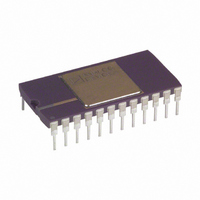
AD565AKD Analog Devices Inc, AD565AKD Datasheet - Page 2

AD565AKD
Manufacturer Part Number
AD565AKD
Description
D/A Converter (D-A) IC
Manufacturer
Analog Devices Inc
Datasheet
1.AD565AJRZ-REEL.pdf
(12 pages)
Specifications of AD565AKD
No. Of Bits
12 Bit
Mounting Type
Through Hole
Interface Type
Serial
Package / Case
24-CDIP
Rohs Status
RoHS non-compliant
Settling Time
250ns
Number Of Bits
12
Data Interface
Parallel
Number Of Converters
1
Voltage Supply Source
Single Supply
Power Dissipation (max)
345mW
Operating Temperature
0°C ~ 70°C
Lead Free Status / RoHS Status
Available stocks
Company
Part Number
Manufacturer
Quantity
Price
AD565A–SPECIFICATIONS
Parameter
DATA INPUTS
TTL or 5 V CMOS
RESOLUTION
OUTPUT
ACCURACY (Error Relative to
DIFFERENTIAL NONLINEARITY
TEMPERATURE COEFFICIENTS
SETTLING TIME TO 1/2 LSB
FULL-SCALE TRANSITION
TEMPERATURE RANGE
POWER REQUIREMENTS
POWER SUPPLY GAIN SENSITIVITY
PROGRAMMABLE OUTPUT RANGES
EXTERNAL ADJUSTMENTS
REFERENCE INPUT
REFERENCE OUTPUT
POWER DISSIPATION
NOTES
1
2
3
Specifications subject to change without notice.
The digital inputs are guaranteed but not tested over the operating temperature range.
The power supply gain sensitivity is tested in reference to a V
For operation at elevated temperatures, the reference cannot supply current for external loads. It, therefore, should be buffered if additional loads are to be supplied.
Input Voltage
Logic Current (Each Bit)
Current
Resistance (Exclusive of Span Resistors)
Offset
Capacitance
Compliance Voltage
Full Scale) 25°C
T
25°C
T
With Internal Reference
All Bits ON-to-OFF or OFF-to-ON
10% to 90% Delay plus Rise Time
90% to 10% Delay plus Fall Time
Operating
Storage
V
V
V
V
Gain Error with Fixed 50 Ω
Bipolar Zero Error with Fixed
Gain Adjustment Range (Figure 2)
Bipolar Zero Adjustment Range
Input Impedance
Voltage
Current (Available for External Loads)
(See Figures 2, 3, 4)
MIN
MIN
CC
EE
CC
EE
Unipolar (All Bits On)
Bit ON Logic “1”
Bit OFF Logic “0”
Bit ON Logic “1”
Bit OFF Logic “0”
Bipolar (All Bits On or Off)
Unipolar
Bipolar (Figure 3, R2 = 50 Ω Fixed)
T
Unipolar Zero
Bipolar Zero
Gain (Full Scale)
Differential Nonlinearity
Resistor for R2 (Figure 2)
50 Ω Resistor for R1 (Figure 3)
, –11.4 to –16.5 V dc
, +11.4 to +16.5 V dc
= –11.4 to –16.5 V dc
MIN
= +11.4 to +16.5 V dc
to T
to T
to T
MAX
MAX
MAX
1
(Pins 13 to 24)
3
2
Min
2.0
–1.6
6
–1.5
MONOTONICITY GUARANTEED
0
–65
± 0.25
± 0.15
15
9.90
1.5
0.8
CC
AD565AJ
, V
Typ
120
35
–2.0
± 1.0
8
0.01
0.05
25
± 1/4
(0.006)
± 1/2
(0.012)
± 1/2
1
5
15
2
250
15
30
3
–12
3
15
0 to +5
–2.5 to +2.5
0 to +10
–5 to +5
–10 to +10
± 0.1
± 0.05
20
10.00
2.5
225
(T
EE
A
of ± 15 V dc.
= 25 C, V
Max
5.5
0.8
300
100
12
–2.4
10
0.05
0.15
+10
(0.012)
(0.018)
2
10
50
400
30
50
+70
+150
5
–18
10
25
25
10.10
345
CC
–2–
1.2
1/2
3/4
3/4
0.25
0.15
= 15 V, V
EE
Min
2.0
–1.6
6
–1.5
MONOTONICITY GUARANTEED
0
–65
± 0.25
± 0.15
15
9.90
1.5
= 15 V, unless otherwise noted.)
0.8
AD565AK
Typ
120
35
–2.0
± 1.0
8
0.01
0.05
25
± 1/8
(0.003)
± 1/4
(0.006)
± 1/4
1
5
10
2
250
15
30
3
–12
3
15
0 to +5
–2.5 to +2.5
0 to +10
–5 to +5
–10 to +10
± 0.1
± 0.05
20
10.00
2.5
225
(0.012)
Max
5.5
0.8
300
100
12
–2.4
10
0.05
0.1
+10
(0.0084)
2
10
20
400
30
50
+70
+150
5
–18
10
25
± 0.1
25
10.10
345
1.2
0.35
1/2
1/2
0.25
Unit
V
V
µA
µA
Bits
mA
mA
kΩ
% of F.S. Range
% of F.S. Range
pF
V
LSB
% of F.S. Range
LSB
% of F.S. Range
LSB
ppm/°C
ppm/°C
ppm/°C
ppm/°C
ns
ns
ns
°C
°C
mA
mA
ppm of F.S./%
ppm of F.S./%
V
V
V
V
V
% of F.S. Range
% of F.S. Range
% of F.S. Range
% of F.S. Range
kΩ
V
mA
mW
REV. E


