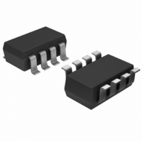
AD5662BRJZ-2500RL7 Analog Devices Inc, AD5662BRJZ-2500RL7 Datasheet - Page 19

AD5662BRJZ-2500RL7
Manufacturer Part Number
AD5662BRJZ-2500RL7
Description
Single 16bit SPI DAC Reset To Midscale
Manufacturer
Analog Devices Inc
Series
nanoDAC™r
Datasheet
1.AD5662BRJZ-2REEL7.pdf
(24 pages)
Specifications of AD5662BRJZ-2500RL7
Design Resources
4 mA to 20 mA Process Control Loop Using AD5662 (CN0009) 16-Bit Fully Isolated Voltage Output Module Using AD5662, ADuM1401, and External Amplifiers (CN0063) 16-Bit Fully Isolated 4 mA to 20 mA Output Module Using AD5662, ADuM1401, and External Amplifiers (CN0064)
Settling Time
8µs
Number Of Bits
16
Data Interface
DSP, MICROWIRE™, QSPI™, Serial, SPI™
Number Of Converters
1
Voltage Supply Source
Single Supply
Power Dissipation (max)
750µW
Operating Temperature
-40°C ~ 125°C
Mounting Type
Surface Mount
Package / Case
SOT-23-8
Lead Free Status / RoHS Status
Lead free / RoHS Compliant
Available stocks
Company
Part Number
Manufacturer
Quantity
Price
Company:
Part Number:
AD5662BRJZ-2500RL7
Manufacturer:
AD
Quantity:
1 000
BIPOLAR OPERATION USING THE AD5662
The AD5662 has been designed for single-supply operation,
but a bipolar output range is also possible using the circuit in
Figure 42. The circuit gives an output voltage range of ±5 V.
Rail-to-rail operation at the amplifier output is achievable using
an AD820 or an OP295 as the output amplifier.
The output voltage for any input code can be calculated as
follows:
where D represents the input code in decimal (0 to 65,535).
With V
This is an output voltage range of ±5 V, with 0x0000 corre-
sponding to a −5 V output, and 0xFFFF corresponding to a
+5 V output.
+5V
V
V
O
O
DD
=
=
= 5 V, R1 = R2 = 10 kΩ,
⎛
⎜
⎝
⎡
⎢
⎣
10μF
V
65
10
DD
Figure 42. Bipolar Operation with the AD5662
,
×
536
D
×
⎛
⎜
⎝
⎞
⎟
⎠
0.1μF
65
−
5
D
,
536
V
V
REF
⎞
⎟
⎠
THREE-WIRE
×
INTERFACE
R1 = 10kΩ
AD5662
⎛
⎜
⎝
SERIAL
R1
R1
SERIAL
+
LOAD
R2
V
V
OUT
FB
⎞
⎟
⎠
−
V
DD
AD5662
AD820/
OP295
R2 = 10kΩ
×
+5V
–5V
Figure 43. Programmable 4–20 mA Process Controller
⎛
⎜
⎝
R2
R1
⎞
⎟
⎠
⎤
⎥
⎦
4.7kΩ
R1
ADJUST
ADJUST
18.5kΩ
20mA
±5V
1.5kΩ
P1
4mA
Rev. A | Page 19 of 24
P2
R2
R3
AD8627
ADR02
USING THE AD5662 AS AN ISOLATED,
PROGRAMMABLE, 4-20 mA PROCESS
CONTROLLER
In many process control system applications, 2-wire current
transmitters are used to transmit analog signals through noisy
environments. These current transmitters use a zero-scale
signal current of 4 mA that can power the transmitter’s signal
conditioning circuitry. The full-scale output signal in these
transmitters is 20 mA. The converse approach to process
control can also be used; a low-power, programmable current
source can be used to control remotely located sensors or
devices in the loop.
A circuit that performs this function is shown in Figure 43.
Using the AD5662 as the controller, the circuit provides a
programmable output current of 4 mA to 20 mA, proportional
to the DAC’s digital code. Biasing for the controller is provided
by the ADR02 and requires no external trim for two reasons:
(1) the ADR02’s tight initial output voltage tolerance and (2)
the low supply current consumption of both the AD8627 and
the AD5662. The entire circuit, including opto-couplers,
consumes less than 3 mA from the total budget of 4 mA. The
AD8627 regulates the output current to satisfy the current
summation at the noninverting node of the AD8627.
For the values shown in Figure 43,
where D = 0 ≤ D ≤ 65535, giving a full-scale output current of
20 mA when the AD5662’s digital code equals 0xFFFF. Offset
trim at 4 mA is provided by P2, and P1 provides the circuit’s
gain trim at 20 mA. These two trims do not interact because
the noninverting input of the AD8627 is at virtual ground. The
Schottky diode, D1, is required in this circuit to prevent loop
supply power-on transients from pulling the noninverting input
of the AD8627 more than 300 mV below its inverting input.
Without this diode, such transients could cause phase reversal
of the AD8627 and possible latch-up of the controller. The loop
supply voltage compliance of the circuit is limited by the maxi-
mum applied input voltage to the ADR02 and is from 12 V to
40 V.
3.3kΩ
R6
100Ω
I
I
R7
OUT
OUT
Q1
2N3904
= 1/
= 0.2435 μA × D + 4 mA
D1
R7 (V
4mA TO 20mA
DAC
× R3 / R1 + V
12V TO 36V
RL
V
LOOP
REF
× R3 / R2 )
AD5662


