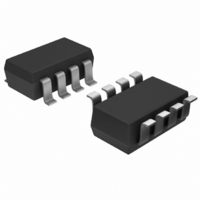
AD5662BRJZ-2500RL7 Analog Devices Inc, AD5662BRJZ-2500RL7 Datasheet - Page 6

AD5662BRJZ-2500RL7
Manufacturer Part Number
AD5662BRJZ-2500RL7
Description
Single 16bit SPI DAC Reset To Midscale
Manufacturer
Analog Devices Inc
Series
nanoDAC™r
Datasheet
1.AD5662BRJZ-2REEL7.pdf
(24 pages)
Specifications of AD5662BRJZ-2500RL7
Design Resources
4 mA to 20 mA Process Control Loop Using AD5662 (CN0009) 16-Bit Fully Isolated Voltage Output Module Using AD5662, ADuM1401, and External Amplifiers (CN0063) 16-Bit Fully Isolated 4 mA to 20 mA Output Module Using AD5662, ADuM1401, and External Amplifiers (CN0064)
Settling Time
8µs
Number Of Bits
16
Data Interface
DSP, MICROWIRE™, QSPI™, Serial, SPI™
Number Of Converters
1
Voltage Supply Source
Single Supply
Power Dissipation (max)
750µW
Operating Temperature
-40°C ~ 125°C
Mounting Type
Surface Mount
Package / Case
SOT-23-8
Lead Free Status / RoHS Status
Lead free / RoHS Compliant
Available stocks
Company
Part Number
Manufacturer
Quantity
Price
Company:
Part Number:
AD5662BRJZ-2500RL7
Manufacturer:
AD
Quantity:
1 000
AD5662
ABSOLUTE MAXIMUM RATINGS
T
Table 3.
Parameter
V
V
V
V
Digital Input Voltage to GND
Operating Temperature Range
Storage Temperature Range
Junction Temperature (T
SOT-23 Package (4-Layer Board)
MSOP Package (4-Layer Board)
Reflow Soldering Peak Temperature
ESD
ESD CAUTION
ESD (electrostatic discharge) sensitive device. Electrostatic charges as high as 4000 V readily accumulate on
the human body and test equipment and can discharge without detection. Although this product features
proprietary ESD protection circuitry, permanent damage may occur on devices subjected to high energy
electrostatic discharges. Therefore, proper ESD precautions are recommended to avoid performance
degradation or loss of functionality.
DD
OUT
FB
REF
A
Industrial (Y Version)
Power Dissipation
θ
θ
θ
SnPb
Pb-free
= 25°C, unless otherwise noted.
to GND
to GND
JA
JA
JC
to GND
to GND
Thermal Impedance
Thermal Impedance
Thermal Impedance
J
max)
−0.3 V to +7 V
−0.3 V to V
−0.3 V to V
−0.3 V to V
−40°C to +125°C
−65°C to +150°C
2 kV
Rating
−0.3 V to V
150°C
(T
119°C/W
141°C/W
44°C/W
240°C
260°C
J
max − T
DD
DD
DD
DD
A
)/θ
+ 0.3 V
+ 0.3 V
+ 0.3 V
+ 0.3 V
JA
Rev. A | Page 6 of 24
Stresses above those listed under Absolute Maximum Ratings
may cause permanent damage to the device. This is a stress
rating only; functional operation of the device at these or any
other conditions above those listed in the operational sections
of this specification is not implied. Exposure to absolute
maximum rating conditions for extended periods may affect
device reliability.


