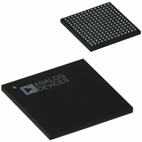
AD6634BBC Analog Devices Inc, AD6634BBC Datasheet - Page 26

AD6634BBC
Manufacturer Part Number
AD6634BBC
Description
IC,RF/Baseband Circuit,CMOS,BGA,196PIN,PLASTIC
Manufacturer
Analog Devices Inc
Series
AD6634r
Datasheet
1.AD6634BCPCB.pdf
(52 pages)
Specifications of AD6634BBC
Rohs Status
RoHS non-compliant
Rf Type
Cellular, CDMA2000, EDGE, GPRS, GSM
Number Of Mixers
1
Voltage - Supply
3 V ~ 3.6 V
Package / Case
196-CSPBGA
Current - Supply
-
Frequency
-
Gain
-
Noise Figure
-
Secondary Attributes
-
Lead Free Status / RoHS Status
Available stocks
Company
Part Number
Manufacturer
Quantity
Price
Company:
Part Number:
AD6634BBC
Manufacturer:
AD
Quantity:
13 888
Part Number:
AD6634BBC
Manufacturer:
ADI/亚德诺
Quantity:
20 000
AD6634
The decimation ratio, M
(all integer values). The frequency response of the filter is given
by the following equations. The gain and pass-band droop of
CIC5 should be calculated by these equations. Both parameters
may be compensated for in the RCF stage.
The scale factor, S
0 and 20. It serves to control the attenuation of the data into the
CIC5 stage in 6 dB increments. For the best dynamic range, S
should be set to the smallest value possible (lowest attenuation)
without creating an overflow condition. This can be safely accom-
plished using the following equation, where OL
MCIC5
10
11
12
13
14
15
16
17
18
19
20
21
22
23
24
25
26
27
28
29
30
31
32
2
3
4
5
6
7
8
9
H z
H f
( )
( )
CIC5
=
=
is a programmable unsigned integer between
2
2
S
S
CIC
CIC
1
–50 dB
10.227
7.924
6.213
5.068
4.267
3.68
3.233
2.881
2.365
2.005
1.863
1.632
1.307
1.245
1.188
1.046
0.934
0.902
0.844
0.818
1
2.598
2.17
1.74
1.536
1.451
1.375
1.137
1.09
1.006
0.969
0.872
CIC5
f
5
SAMP
5
+
+
5
5
, may be programmed from 2 to 32
1
2
sin
−
1
≤
sin
−
z
N
f
π
−
CLK
z
M
CH
π
−
M
CIC
1
Table IV. SSB CIC5 Alias Rejection Table (f
f
f
CIC
5
SAMP
SAMP
f
5
5
–60 dB
8.078
6.367
5.022
4.107
3.463
2.989
2.627
2.342
2.113
1.924
1.765
1.631
1.516
1.416
1.328
1.25
1.181
1.119
1.064
1.013
0.967
0.925
0.887
0.852
0.819
0.789
0.761
0.734
0.71
0.687
0.666
×
2
2
f
rCIC2
5
is the largest
CIC5
–70 dB
6.393
5.11
4.057
3.326
2.808
2.425
2.133
1.902
1.716
1.563
1.435
1.326
1.232
1.151
1.079
1.016
0.96
0.91
0.865
0.824
0.786
0.752
0.721
0.692
0.666
0.641
0.618
0.597
0.577
0.559
0.541
–26–
fraction of full scale possible at the input to this filter stage. This
value is output from the rCIC2 stage then pipelined into the CIC5.
The output rate of this stage is given by the equation below.
CIC5 Rejection
Table IV illustrates the amount of bandwidth in percentage of
the clock rate that can be protected with various decimation
rates and alias rejection specifications. The maximum input rate
into the CIC5 is 80 MHz when the rCIC2 decimates by 1. As in
the Table III, these are the one-half bandwidth characteristics of
the CIC5. Notice that the CIC5 stage can protect a much wider
band to any given rejection.
This table helps to calculate an upper bound on decimation,
M
CIC5
, given the desired filter characteristics.
OL
–80 dB
5.066
4.107
3.271
2.687
2.27
1.962
1.726
1.54
1.39
1.266
1.162
1.074
0.998
0.932
0.874
0.823
0.778
0.737
0.701
0.667
0.637
0.61
0.584
0.561
0.54
0.52
0.501
0.484
0.468
0.453
0.439
S
CIC
rCIC
5
SAMP2
=
2
ceil
=
= 1)
(
2
M
S
f
log
CIC
SAMP
CIC
5
2
5
+
(
5
–90 dB
4.008
3.297
2.636
2.17
1.836
1.588
1.397
1.247
1.125
1.025
0.941
0.87
0.809
0.755
0.708
0.667
0.63
0.597
0.568
0.541
0.516
0.494
0.474
0.455
0.437
0.421
0.406
0.392
0.379
0.367
0.355
5
5
M
)
=
×
CIC
OL
M
f
SAMP
5
CIC
5
rCIC
×
5
2
OL
2
rCIC
–100 dB
3.183
2.642
2.121
1.748
1.48
1.281
1.128
1.007
0.909
0.828
0.76
0.703
0.653
0.61
0.572
0.539
0.509
0.483
0.459
0.437
0.417
0.399
0.383
0.367
0.353
0.34
0.328
0.317
0.306
0.297
0.287
2
)
–
5
REV. 0


