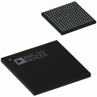
AD6634BBC Analog Devices Inc, AD6634BBC Datasheet - Page 34

AD6634BBC
Manufacturer Part Number
AD6634BBC
Description
IC,RF/Baseband Circuit,CMOS,BGA,196PIN,PLASTIC
Manufacturer
Analog Devices Inc
Series
AD6634r
Datasheet
1.AD6634BCPCB.pdf
(52 pages)
Specifications of AD6634BBC
Rohs Status
RoHS non-compliant
Rf Type
Cellular, CDMA2000, EDGE, GPRS, GSM
Number Of Mixers
1
Voltage - Supply
3 V ~ 3.6 V
Package / Case
196-CSPBGA
Current - Supply
-
Frequency
-
Gain
-
Noise Figure
-
Secondary Attributes
-
Lead Free Status / RoHS Status
Available stocks
Company
Part Number
Manufacturer
Quantity
Price
Company:
Part Number:
AD6634BBC
Manufacturer:
AD
Quantity:
13 888
Part Number:
AD6634BBC
Manufacturer:
ADI/亚德诺
Quantity:
20 000
AD6634
PxCH[1:0]
The 16-bit interleaved format provides I and Q data for each
output sample on back-to-back PCLK cycles. Both I and Q
words consist of the full port width of 16 bits. Data output is
triggered on the rising edge of PCLK when both REQ and ACK
are asserted. I data is output during the first PCLK cycle; and the
PAIQ and PBIQ output indicator pins are set high to indicate
that I data is on the bus. Q data is output during the subsequent
PCLK cycle; and the PAIQ and PBIQ output indicator pins are
low during this cycle.
The 8-bit concurrent format provides eight bits of I data and
eight bits of Q data simultaneously during one PCLK cycle, also
triggered on the rising edge of PCLK. The I byte occupies the
most significant byte of the port, while the Q byte occupies the
least significant byte. The PAIQ and PBIQ output indicator
pins are set high during the PCLK cycle. Note that if data from
multiple channels are output consecutively, the PAIQ and PBIQ
output indicator pins will remain high until data from all channels
has been output.
The PACH[1:0] and PBCH[1:0] pins provide a 2-bit binary value
indicating the source channel of the data currently being output.
Care should be taken to read data from the port as soon as possible.
If not, the sample will be overwritten when the next new data
PxCH[1:0]
Px[15:0]
Px[15:0]
PxACK
PxREQ
PxACK
PxREQ
PCLK
PCLK
PxlQ
PxlQ
Figure 37. Channel Mode 8I/8Q Parallel Format
Figure 36. Channel Mode Interleaved Format
t
t
t
t
DPREQ
DPP
DPIQ
DPCH
I[15:0]
PxCH[1:0] = CHANNEL #
t
t
t
t
I[15:8]; Q[7:0]
DPREQ
DPP
DPIQ
DPCH
PxCH[1:0] =
CHANNEL #
Q[15:0]
–34–
sample arrives. This occurs on a per-channel basis; i.e., a
channel 0 sample will only be overwritten by a new channel 0
sample, and so on.
The order of data output is dependent on when data arrived at
the port, which is a function of total decimation rate, Start-Hold-Off
values, and so on. Priority order is, from highest to lowest,
channels 0, 1, 2, 3.
AGC Mode
Parallel port channel mode is selected by clearing Bit 0 of
addresses 0x1A and 0x1C for parallel ports A and B, respectively.
I and Q data output in AGC mode are output from the AGC, not
the individual channels. Each AGC receives data from only two
AD6634 channels; AGC A accepts data from channels 0 and 1,
while AGC B accepts data from channels 2 and 3. Each pair of
channels is required to be configured such that the generation of
output samples from the channels is out of phase (by typically
180 degrees). Each parallel port can provide data from either one
or both AGCs. Bits 1 and 2 of register addresses 0x1A (port A)
and 0x1C (port B) control the inclusion of data from AGCs
A and B, respectively.
AGC mode provides only one I and Q format, which is similar
to the 16-bit interleaved format of Channel mode. When both
REQ and ACK are asserted, the next rising edge of PCLK
triggers the output of a 16-bit AGC I word for one PCLK cycle.
The PAIQ and PBIQ output indicator pins are high during this
cycle, and low otherwise. A 16-bit AGC Q word is provided
during the subsequent PCLK cycle. If the AGC gain word has
been updated since the last sample, a 12-bit RSSI (Receive Signal
Strength Indicator) word is provided during the PCLK cycle
following the Q word on 12 MSBs of the parallel port data pins.
The RSSI word is the bit-inverse of the Signal Gain word used
in the Gain multiplier of the AGC.
The data provided by the PACH[1:0] and PBCH[1:0] pins in
AGC mode is different than that provided in Channel mode. In
AGC mode, PACH[0] and PBCH[0] indicate the AGC source of
the data currently being output (0 = AGC A, 1 = AGC B). PACH[1]
and PBCH[1] indicate whether the current data is an I/Q word or
an AGC RSSI word (0 = I/Q word, 1 = AGC RSSI word). The
two different AGC outputs are shown in Figures 38 and 39.
PxCH[1:0]
Px[15:0]
PxACK
PxREQ
PCLK
PxlQ
Figure 38. AGC Output with No RSSI Word
t
t
t
t
I[15:0]
DPREQ
DPP
DPIQ
DPCH
PxCH[0] = AGC #
PxCH[1] = 0
Q[15:0]
REV. 0


