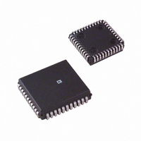
AD664KPZ Analog Devices Inc, AD664KPZ Datasheet - Page 10

AD664KPZ
Manufacturer Part Number
AD664KPZ
Description
IC - 12-BIT QUAD DAC IC
Manufacturer
Analog Devices Inc
Datasheet
1.AD664JNZ-BIP.pdf
(20 pages)
Specifications of AD664KPZ
Settling Time
8µs
Number Of Bits
12
Data Interface
Parallel
Number Of Converters
4
Voltage Supply Source
Dual ±
Power Dissipation (max)
525mW
Operating Temperature
0°C ~ 70°C
Mounting Type
Surface Mount
Package / Case
44-PLCC
Lead Free Status / RoHS Status
Lead free / RoHS Compliant
Available stocks
Company
Part Number
Manufacturer
Quantity
Price
Company:
Part Number:
AD664KPZ
Manufacturer:
ANAREN
Quantity:
1 000
AD664
occupies the topmost eight bits of the input word. The last four
bits of the input word are “don’t cares.”
Figure 15 shows the format of the MODE SELECT word. The
first four bits determine the gain range of the DAC. When set to
be a gain of 1, the output of the DAC spans a voltage of 1 times
the reference. When set to a gain of 2, the output of the DAC
spans a voltage of 2 times the reference.
The next four bits determine the mode of the DAC. When set to
UNIPOLAR, the output goes from 0 to REF or 0 to 2 REF.
When the BIPOLAR mode is selected, the output goes from
–REF/2 to REF/2 or –REF to REF.
Load and Update Mode of One DAC
In this next example, the object is to load new mode informa-
tion for one of the DACs into the first rank of latches and then
immediately update the second rank. This is done by putting the
new mode information (8-bit word length) onto the databus.
Then MS and LS are pulled low. Following that, CS is pulled
low. This loads the mode information into the first rank of
latches. LS is then brought high. This action updates the second
rank of latches (and, therefore, the DAC outputs). The load
cycle ends when CS is brought high.
In reality, this load cycle really updates the modes of all the
DACs, but the effect is to only change the modes of those
DACs whose mode select information has actually changed.
Figure 16b. Load and Update Mode of One DAC Timing
Figure 16a. Load and Update Mode of One DAC
Figure 15. Mode Select Word Format
SYMBOL
t
t
t
t
t
t
t
*FOR t
MS
LS
DS
LW
CH
DH
MH
INCREASED BY THE SAME AMOUNT THAT
t
LS
*
IS GREATER THAN 0 ns.
LS
> 0, THE WIDTH OF LS MUST BE
25 C
MIN (ns)
0
0
0
60
70
0
0
T
MIN (ns)
0
0
0
70
80
0
0
MIN
to T
MAX
–10–
Preloading the Mode Select Register
Mode data can be written into the first rank of the mode select
latch without changing the modes currently being used. This
feature is useful when a user wants to preload new mode infor-
mation in anticipation of strobing that in at a future time. Fig-
ure 17 illustrates the correct sequence and timing of control
signals to accomplish this task.
This allows the user to “preload” the data to a DAC and strobe
it into the output latch at some future time. The user could do
this by reproducing the sequence of signals illustrated in Figures
17c and 17d.
Transparent Operation (44-Pin Versions)
Transparent operation allows data from the inputs of the
AD664 to be transferred into the DAC registers without the
intervening step of being latched into the first rank of latches.
Two modes of transparent operation exist, the “partially trans-
parent” mode and a “fully transparent” mode. In the “partially
transparent” mode, one of the DACs is transparent while the
remaining three continue to use the data latched into their
respective input registers. Both modes require a 12-bit wide
input word!
Figure 17d. Update Second Rank of Mode Select Latch
Timing
Figure 17c. Update Second Rank of Mode Select Latch
Figure 17b. Preload Mode Select Register Timing
Figure 17a. Preload Mode Select Register
INPUT/OUTPUT
QS0,QS1,QS2
___
SYMBOL
t
t
t
ADDRESS
MS
MH
W
DS0,DS1
DATA
BITS
___
___
__
MS
CS
__
1
0
1
0
25 C
MIN (ns)
0
0
80
t
MS
T
MIN (ns)
0
0
100
t
MIN
W
to T
MAX
t
MH
REV. C


