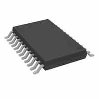
AD7190BRUZ-REEL Analog Devices Inc, AD7190BRUZ-REEL Datasheet - Page 26

AD7190BRUZ-REEL
Manufacturer Part Number
AD7190BRUZ-REEL
Description
2ch UltraLow Noise 24Bit SD ADC IC.
Manufacturer
Analog Devices Inc
Datasheet
1.AD7190BRUZ.pdf
(40 pages)
Specifications of AD7190BRUZ-REEL
Design Resources
Precision Weigh Scale Design Using AD7190 with Internal PGA (CN0102)
Number Of Bits
24
Sampling Rate (per Second)
4.8k
Data Interface
DSP, MICROWIRE™, QSPI™, Serial, SPI™
Number Of Converters
1
Voltage Supply Source
Analog and Digital
Operating Temperature
-40°C ~ 105°C
Mounting Type
Surface Mount
Package / Case
24-TSSOP (0.173", 4.40mm Width)
Lead Free Status / RoHS Status
Lead free / RoHS Compliant
Available stocks
Company
Part Number
Manufacturer
Quantity
Price
Company:
Part Number:
AD7190BRUZ-REEL
Manufacturer:
ADI
Quantity:
1 000
Part Number:
AD7190BRUZ-REEL
Manufacturer:
ADI/亚德诺
Quantity:
20 000
AD7190
ADC CIRCUIT INFORMATION
OVERVIEW
The AD7190 is an ultralow noise ADC that incorporates a
∑-Δ modulator, a buffer, PGA, and on-chip digital filtering
intended for the measurement of wide dynamic range signals
such as those in pressure transducers, weigh scales, and strain
gauge applications.
The part can be configured to have two differential inputs or four
pseudo differential inputs that can be buffered or unbuffered.
Figure 18 shows the basic connections required to operate the part.
FILTER, OUTPUT DATA RATE, SETTLING TIME
A ∑-Δ ADC consists of a modulator followed by a digital filter.
The AD7190 has two filter options: a sinc
filter. The filter is selected using the SINC3 bit in the mode
register. When SINC3 is set to 0 (default value), the sinc
selected. The sinc
At low output data rates (<1 kHz), the noise-free resolution is
comparable for the two filter types. However, at the higher
output data rates, the sinc
resolution.
The sinc
While the notch positions are not affected by the order of the
filter, the higher order filter has wider notches, which leads to
better rejection in the band (±1 Hz) around the notches. It also
gives better stop-band attenuation. The benefit of the sinc
is its lower settling time for the same output data rate.
Chop Disabled
The output data rate (the rate at which conversions are available
on a single channel when the ADC is continuously converting)
is equal to
f
ADC
4
= f
filter also leads to better 50 Hz and 60 Hz rejection.
CLK
/(1024 × FS[9:0])
3
filter is selected when SINC3 is set to 1.
OUT–
IN+
IN–
4
filter gives better noise free
5V
OUT+
3
REFIN1(+)
AIN1
AIN2
AIN3
AIN4
AINCOM
REFIN1(–)
BPDSW
filter and a sinc
AGND
MUX
AGND
Figure 18. Basic Connection Diagram
AGND
AV
4
filter is
DD
AV
3
4
filter
AD7190
DD
Rev. B | Page 26 of 40
SENSOR
TEMP
PGA
MCLK1 MCLK2
CIRCUITRY
where:
f
f
FS[9:0] is the decimal equivalent of Bit FS9 to Bit FS0 in the
mode register.
The output data rate can be programmed from 4.7 Hz to 4800 Hz;
that is, FS[9:0] can have a value from 1 to 1023.
The previous equation is valid for both the sinc
filters. The settling time for the sinc
Whereas the settling time for the sinc
Figure 19 and Figure 20 show the frequency response of the sinc
and sinc
CLOCK
ADC
CLK
= master clock (4.92 MHz nominal).
is the output data rate.
t
t
DV
SETTLE
SETTLE
–100
–10
–20
–30
–40
–50
–60
–70
–80
–90
ADC
DD
Σ-Δ
0
3
Figure 19. Sinc
0
filters, respectively, for an output data rate of 50 Hz.
DGND
= 4/f
= 3/f
P0/REFIN2(–) P1/REFIN2(+)
ADC
ADC
25
INTERFACE
CONTROL
SERIAL
LOGIC
4
REFERENCE
AND
Filter Response (50 Hz Output Data Rate)
DETECT
50
FREQUENCY (Hz)
75
DOUT/RDY
DIN
SCLK
CS
SYNC
P3
P2
4
filter is equal to
3
filter is equal to
100
3
125
and sinc
150
4
4


