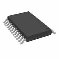
AD7190BRUZ-REEL Analog Devices Inc, AD7190BRUZ-REEL Datasheet - Page 37

AD7190BRUZ-REEL
Manufacturer Part Number
AD7190BRUZ-REEL
Description
2ch UltraLow Noise 24Bit SD ADC IC.
Manufacturer
Analog Devices Inc
Datasheet
1.AD7190BRUZ.pdf
(40 pages)
Specifications of AD7190BRUZ-REEL
Design Resources
Precision Weigh Scale Design Using AD7190 with Internal PGA (CN0102)
Number Of Bits
24
Sampling Rate (per Second)
4.8k
Data Interface
DSP, MICROWIRE™, QSPI™, Serial, SPI™
Number Of Converters
1
Voltage Supply Source
Analog and Digital
Operating Temperature
-40°C ~ 105°C
Mounting Type
Surface Mount
Package / Case
24-TSSOP (0.173", 4.40mm Width)
Lead Free Status / RoHS Status
Lead free / RoHS Compliant
Available stocks
Company
Part Number
Manufacturer
Quantity
Price
Company:
Part Number:
AD7190BRUZ-REEL
Manufacturer:
ADI
Quantity:
1 000
Part Number:
AD7190BRUZ-REEL
Manufacturer:
ADI/亚德诺
Quantity:
20 000
The AD7190 gives the user access to the on-chip calibration
registers, allowing the microprocessor to read the calibration
coefficients of the device and also to write its own calibration
coefficients from prestored values in the EEPROM. A read of
the registers can be performed at any time. However, the ADC
must be placed in power-down or idle mode when writing to
the registers. The values in the calibration registers are 24-bits
wide. The span and offset of the part can also be manipulated
using the registers.
GROUNDING AND LAYOUT
Because the analog inputs and reference inputs are differential,
most of the voltages in the analog modulator are common-
mode voltages. The high common-mode rejection of the part
removes common-mode noise on these inputs. The analog and
digital supplies to the AD7190 are independent and separately
pinned out to minimize coupling between the analog and
digital sections of the device. The digital filter provides
rejection of broadband noise on the power supplies, except at
integer multiples of the modulator sampling frequency.
Connect an R-C filter to each analog input pin to provide
rejection at the modulator sampling frequency. A 100 Ω
resistor in series with each analog input, a 0.1 μF capacitor
between the analog inputs along with a 0.01 μF capacitor from
each analog input to AGND is advised. The digital filter also
removes noise from the analog and reference inputs provided
these noise sources do not saturate the analog modulator. As a
result, the AD7190 is more immune to noise interference than a
conventional high resolution converter. However, because the
resolution of the AD7190 is so high and the noise levels from
the converter so low, care must be taken with regard to grounding
and layout.
The printed circuit board (PCB) that houses the ADC must be
designed so that the analog and digital sections are separated
and confined to certain areas of the board. This facilitates the
use of ground planes that can be easily separated. A minimum
etch technique is generally best for ground planes because it
gives the best shielding.
Although the AD7190 has separate pins for analog and digital
ground, the AGND and DGND pins are tied together internally
via the substrate. Therefore, the user must not tie these two
Rev. B | Page 37 of 40
pins to separate ground planes unless the ground planes are
connected together near the AD7190.
In systems in which the AGND and DGND are connected
somewhere else in the system (that is, the power supply of the
system), they should not be connected again at the AD7190
because a ground loop results. In these situations, it is
recommended that ground pins of the AD7190 be tied to the
AGND plane.
In any layout, the user must keep in mind the flow of currents
in the system, ensuring that the paths for all currents are as close
as possible to the paths the currents took to reach their destin-
ations. Avoid forcing digital currents to flow through the AGND.
Avoid running digital lines under the device because this
couples noise onto the die and allow the analog ground plane to
run under the AD7190 to prevent noise coupling. The power
supply lines to the AD7190 must use as wide a trace as possible
to provide low impedance paths and reduce the effects of
glitches on the power supply line. Shield fast switching signals
like clocks with digital ground to prevent radiating noise to
other sections of the board, and never run clock signals near the
analog inputs. Avoid crossover of digital and analog signals.
Run traces on opposite sides of the board at right angles to each
other. This reduces the effects of feedthrough through the
board. A microstrip technique is by far the best but is not
always possible with a double-sided board. In this technique,
the component side of the board is dedicated to ground planes,
whereas signals are placed on the solder side.
Good decoupling is important when using high resolution ADCs.
Decouple all analog supplies with 10 μF tantalum in parallel with
0.1 μF capacitors to AGND. To achieve the best from these
decoupling components, place them as close as possible to the
device, ideally right up against the device. Decouple all logic chips
with 0.1 μF ceramic capacitors to DGND. In systems in which a
common supply voltage is used to drive both the AV
of the AD7190, it is recommended that the system AV
be used. For this supply, place the recommended analog supply
decoupling capacitors between the AV
AGND and the recommended digital supply decoupling
capacitor between the DV
DD
pin of the AD7190 and DGND.
DD
pin of the AD7190 and
DD
AD7190
and DV
DD
supply
DD


