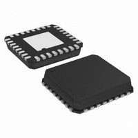
AD8193ACPZ-R7 Analog Devices Inc, AD8193ACPZ-R7 Datasheet - Page 6

AD8193ACPZ-R7
Manufacturer Part Number
AD8193ACPZ-R7
Description
IC,Telecom Switching Circuit,LLCC,32PIN,PLASTIC
Manufacturer
Analog Devices Inc
Datasheet
1.AD8193ACPZ-R7.pdf
(16 pages)
Specifications of AD8193ACPZ-R7
Function
Switch
Circuit
1 x 2:1
Voltage Supply Source
Single Supply
Voltage - Supply, Single/dual (±)
3 V ~ 3.6 V
Current - Supply
50mA
Operating Temperature
-40°C ~ 85°C
Mounting Type
Surface Mount
Package / Case
32-LFCSP
Lead Free Status / RoHS Status
Lead free / RoHS Compliant
AD8193
TYPICAL PERFORMANCE CHARACTERISTICS
T
data rate = 2.25 Gbps, TMDS outputs terminated with external 50 Ω resistors to 3.3 V, unless otherwise noted.
A
= 27°C, AVCC = 3.3 V, VTTI = 3.3 V, VTTO = 3.3 V, AVEE = 0 V, differential input swing = 1000 mV, pattern = PRBS 2
Figure 5. Rx Eye Diagram at TP2 (Cable = 2 m, 30 AWG)
Figure 6. Rx Eye Diagram at TP2 (Cable = 6 m, 24 AWG)
REFERENCE EYE DIAGRAM AT TP1
0.125UI/DIV AT 2.25Gbps
0.125UI/DIV AT 2.25Gbps
GENERATOR
PATTERN
DIGITAL
Figure 4. Test Circuit Diagram for Rx Eye Diagrams
TP1
Rev. 0 | Page 6 of 16
HDMI CABLE
Figure 7. Rx Eye Diagram at TP3 (Cable = 2 m, 30 AWG)
Figure 8. Rx Eye Diagram at TP3 (Cable = 6 m, 24 AWG)
TP2
EVALUATION
AD8193
BOARD
0.125UI/DIV AT 2.25Gbps
0.125UI/DIV AT 2.25Gbps
SMA COAX CABLE
TP3
SERIAL DATA
ANALYZER
7
− 1,


