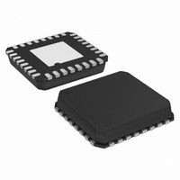
AD8193ACPZ-R7 Analog Devices Inc, AD8193ACPZ-R7 Datasheet - Page 9

AD8193ACPZ-R7
Manufacturer Part Number
AD8193ACPZ-R7
Description
IC,Telecom Switching Circuit,LLCC,32PIN,PLASTIC
Manufacturer
Analog Devices Inc
Datasheet
1.AD8193ACPZ-R7.pdf
(16 pages)
Specifications of AD8193ACPZ-R7
Function
Switch
Circuit
1 x 2:1
Voltage Supply Source
Single Supply
Voltage - Supply, Single/dual (±)
3 V ~ 3.6 V
Current - Supply
50mA
Operating Temperature
-40°C ~ 85°C
Mounting Type
Surface Mount
Package / Case
32-LFCSP
Lead Free Status / RoHS Status
Lead free / RoHS Compliant
THEORY OF OPERATION
INTRODUCTION
The primary function of the AD8193 is to switch the high speed
signals from one of two (HDMI or DVI) single-link sources to
one output. Each source group consists of four differential, high
speed channels. The four high speed channels include a data-
word clock and three Transition Minimized Differential Signaling
(TMDS) data channels running at 10× the data-word clock
frequency for data rates up to 2.25 Gbps. All four high speed
channels of the AD8193 are identical; that is, the pixel clock can
be run on any of the four TMDS channels. The AD8193 does
not provide switching of the low speed DDC and CEC signals.
The AD8193 is a buffered TMDS switch with low added jitter;
the output pins are electrically isolated from the inputs. Because
the AD8193 is a TMDS-only switch, a complete HDMI switch
solution requires another component to switch the low speed
DDC channels. Several low cost CMOS switches can be used
along with the AD8193 to make an HDMI 1.3-compliant 2:1
link switch. The requirements for such a switch are as follows:
•
•
•
A reference design that incorporates the AD8193 and a low cost
CMOS switch is described in more detail in the Evaluation
Board section.
In addition to the AD8193, Analog Devices, Inc., offers several
HDMI switches with integrated DDC, in a variety of form
factors.
Low input capacitance. The HDMI 1.3 specification limits
the total DDC link capacitance for an HDMI sink to less
than 50 pF. This 50 pF limit includes the HDMI connector,
the PCB, the capacitance of the CMOS switch, and what-
ever capacitance is seen at the input of the HDMI receiver.
Low channel on resistance (R
resistance degrade the quality of the DDC signals.
An appropriate form factor to switch the DDC and HPD
signals as necessary.
ON
). Switches with high on
Rev. 0 | Page 9 of 16
INPUT CHANNELS
Each high speed input differential pair terminates to the
3.3 V VTTI power supply through a pair of single-ended 50 Ω
on-chip resistors, as shown in Figure 19. These matched on-
chip terminations absorb reflections on the input TMDS
channels, properly terminating the inputs and improving
overall system signal integrity.
The input termination resistors all have series switches, as
shown in Figure 19. The state of these switches is determined by
the S_SEL signal, which also controls the input selection. The
termination switches for the selected input channel are closed
(terminations present), whereas the termination switches for
the unselected input are open (high-Z inputs).
No specific cable length is suggested for use with the AD8193
because cable performance varies widely between manufactur-
ers. For a 24 AWG reference cable, the AD8193 can operate
with more than 20 m of input cable at data rates equivalent to
1080i, more than 10 meters at 1080p, and more than 6 meters at
1080p, 12-bit color.
IN_xx
IP_xx
Figure 19. High Speed Input Simplified Schematic
AVEE
VTTI
50Ω
50Ω
Rx
AD8193


