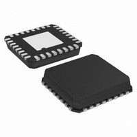
AD8376ACPZ-R7 Analog Devices Inc, AD8376ACPZ-R7 Datasheet - Page 12

AD8376ACPZ-R7
Manufacturer Part Number
AD8376ACPZ-R7
Description
If Cellular Dual DGA
Manufacturer
Analog Devices Inc
Datasheet
1.AD8376ACPZ-R7.pdf
(24 pages)
Specifications of AD8376ACPZ-R7
Design Resources
Using AD8376 to Drive Wide Bandwidth ADCs for High IF AC-Coupled Appls (CN0002) High Performance, Dual Channel IF Sampling Receiver (CN0140)
Amplifier Type
Variable Gain
Number Of Circuits
2
Output Type
Differential
Slew Rate
5000 V/µs
-3db Bandwidth
700MHz
Current - Input Bias
900nA
Current - Supply
250mA
Voltage - Supply, Single/dual (±)
4.5 V ~ 5.5 V
Operating Temperature
-40°C ~ 85°C
Mounting Type
Surface Mount
Package / Case
32-LFCSP
Lead Free Status / RoHS Status
Lead free / RoHS Compliant
Current - Output / Channel
-
Gain Bandwidth Product
-
Voltage - Input Offset
-
Lead Free Status / RoHS Status
Lead free / RoHS Compliant
Other names
AD8376ACPZ-R7TR
Available stocks
Company
Part Number
Manufacturer
Quantity
Price
Company:
Part Number:
AD8376ACPZ-R7
Manufacturer:
Maxim
Quantity:
26
Part Number:
AD8376ACPZ-R7
Manufacturer:
ADI/亚德诺
Quantity:
20 000
CIRCUIT DESCRIPTION
BASIC STRUCTURE
The AD8376 is a dual differential variable gain amplifier with
each amplifier consisting of a 150 Ω digitally controlled passive
attenuator followed by a highly linear transconductance
amplifier.
VCM
Input System
The dc voltage level at the inputs of the AD8376 is set by an
internal voltage reference circuit to about 2 V. This reference is
accessible at VCMA and VCMB and can be used to source or
sink 100 μA. For cases where a common-mode signal is applied
to the inputs, such as in a single-ended application, an external
capacitor between VCMA/VCMB and ground is required. The
capacitor improves the linearity performance of the part in this
mode. This capacitor should be sized to provide a reactance of
10 Ω or less at the lowest frequency of operation. If the applied
common-mode signal is dc, its amplitude should be limited to
0.25 V from VCMA/VCMB (VCMA or VCMB ± 0.25 V). Each
device can be powered down by pulling the ENBA or ENBB pin
down to below 0.8 V. In the powered down mode, the total
current reduces to 3 mA (typical). The dc level at the inputs and
at VCMA/VCMB remains at about 2 V, regardless of the state of
the ENBA of ENBB pin.
Output Amplifier
The gain is based on a 150 Ω differential load and varies as R
changed per the following equations:
and
AD8376
IP+
IP–
Voltage Gain = 20 × (log(R
Power Gain = 10 × (log(R
ATTENUATOR
Figure 33. Simplified Schematic
1/2 AD8376
MUX BUFFERS
A0 TO A4
DIGITAL
SELECT
L
/150) + 2)
L
/150) + 1)
gm CORE
AMP
OP+
OP–
Rev. A | Page 12 of 24
L
is
The dependency of the gain on the load is due to the open-
collector architecture of the output stage.
The dc current to the outputs of each amplifier is supplied
through two external chokes. The inductance of the chokes and
the resistance of the load determine the low frequency pole of
the amplifier. The parasitic capacitance of the chokes adds to
the output capacitance of the part. This total capacitance in
parallel with the load resistance sets the high frequency pole of
the device. Generally, the larger the inductance of the choke, the
higher its parasitic capacitance. Therefore, the value and type of
the choke should be chosen keeping this trade-off in mind.
For operation frequency of 15 MHz to 700 MHz driving a
150 Ω load, 1 μH chokes with SRF of 160 MHz or higher are
recommended (such as 0805LS-102XJBB from Coilcraft).
The supply current of each amplifier consists of about 50 mA
through the VCC pin and 80 mA through the two chokes
combined. The latter increases with temperature at about
2.5 mA per 10°C.
Each amplifier has two output pins for each polarity, and they
are oriented in an alternating fashion. When designing the
board, care should be taken to minimize the parasitic capaci-
tance due to the routing that connects the corresponding
outputs together. A good practice is to avoid any ground or
power plane under this routing region and under the chokes to
minimize the parasitic capacitance.
Gain Control
Two independent 5-bit binary codes change each attenuator
setting in 1 dB steps such that the gain of each amplifier
changes from +20 dB (Code 0) to −4 dB (Code 24 and higher).
The noise figure of each amplifier is about 8 dB at maximum
gain setting, and it increases as the gain is reduced. The increase
in noise figure is equal to the reduction in gain. The linearity of
the part measured at the output is first-order independent of
the gain setting. From 0 dB to 20 dB gain, OIP3 is approximately
50 dBm into 150 Ω load at 140 MHz (3 dBm per tone). At gain
settings below 0 dB, it drops to approximately 45 dBm.


